About the other three operation modes of BJT, and some non-ideal effects, including the Early effect, base punchthrough, and breakdown.
Reverse Active/Cutoff/Saturation Modes
- Reverse active mode: when the base-emitter junction is reverse biased and the base-collector junction is forward biased, electrons are injected from the collector to the base, then to the emitter. Operation is similar to forward active mode
- The BJT still functions as a switch, which is controlled by the base-collector voltage
- But the doping is not optimized for this mode, electron injection from the collector to the base has to be accomplished by a large hole current from the base to the collector
- Like using a large amount of running water to control the water flow in a small pipe
- Cutoff mode: when both the base-emitter junction and the base-collector junction are reverse biased, no current can flow through the junction. The connection between any two terminals of the BJT can be considered as open circuit
- Saturation mode: when both the base-emitter junction and the base-collector junction are forward biased, both emitter and collector inject electrons into the base
- The minority carrier concentration in the base represents the superposition of the forward active and the reverse active cases, and its slope indicates the net current flow
- We can calculate the carrier concentrations at the edges of the depletion regions of the base near the emitter and collector as:
- If
- Excess electrons at the base will recombine with holes, resulting a base hole current
- The base hole current will flow to both the emitter and collector, given by the slope of the minority carrier concentration at the emitter and the collector
- The currents are mainly hole currents from the base to both the emitter and collector
- When
- Excess electrons at the base will recombine with holes, resulting a base hole current
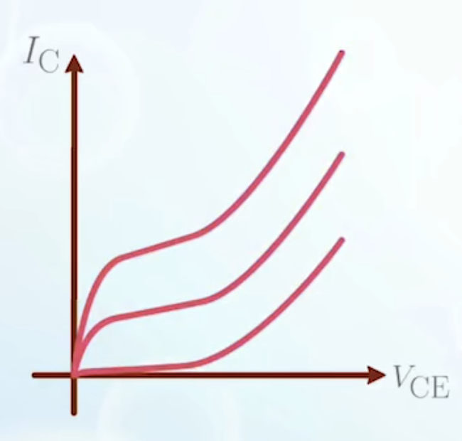
Current-Voltage Characteristics in the Saturation Mode
- From the forward active mode, we decrease
- Further reduction of
- The hole current from the base to the collector increases, and contributes to a negative collector current that subtracts from the original collector current
- The collector current in the
- From the device perspective, the boundary between the forward active mode and the saturation mode is the point where
- Measurement results show that
- Because carrier injection follows exponential scale instead of linear scale
- For example
- The electron injection from the collector to the base can be considered minimal, and the characteristics still follow those of the forward active mode
- The drop in
- Based on the observed data,
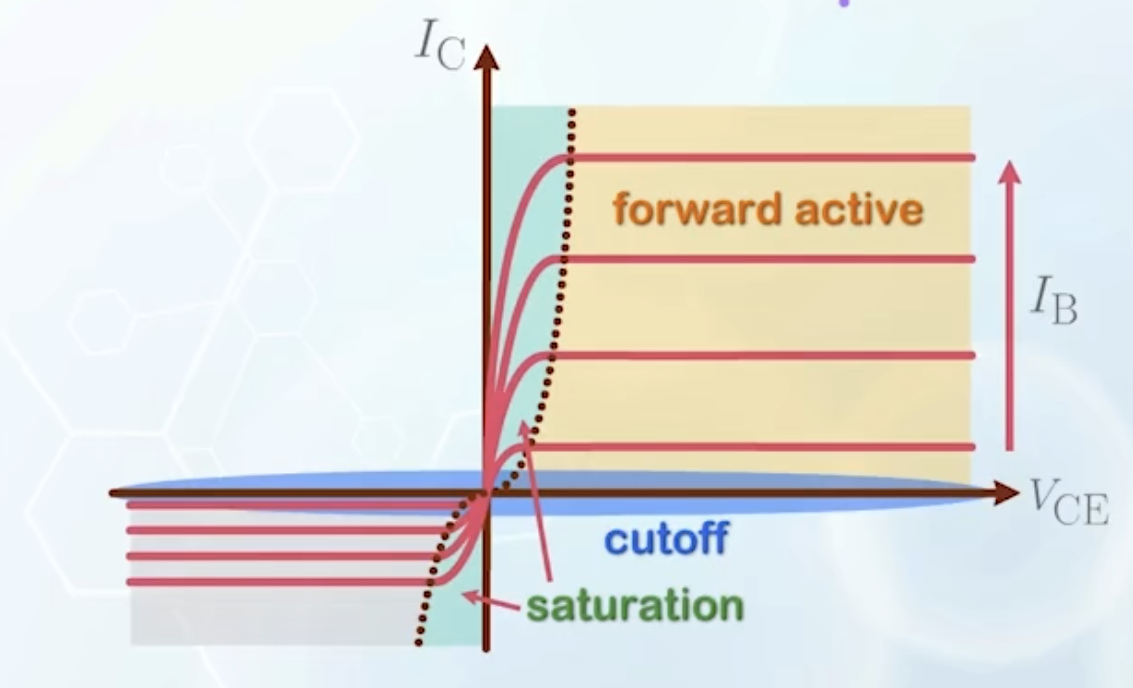
Difference between BJT and MOSFET Saturation Regions
The saturation region of BJT is different from that of MOSFET. The saturation region of BJT corresponds to the linear region of MOSFET, while the saturation region of MOSFET corresponds to the forward active region of BJT.
The Early Effect
Ideally, the collector voltage does not affect the collector current, thus
The collector current is given by the slope of minority carrier concentration at the base
When the collector voltage increases
leading to a finite slope in the
The characteristics are similar to the superposition of a BJT and a resistor in parallel, creating a permanent collector to emitter leakage path, hurting the gain of the transistor
The resistor is called the output resistance
If all collector current at different
The slope is given by
Because
The output resistance can be expressed as
Base Punchthrough
The early effect reduces the gain of the BJT, and should be minimized. This can be done if the change in
- Easiest way: increase the base width
- Not applicable, because it will increase more recombination in the base, reducing
- Not applicable, because it will increase more recombination in the base, reducing
- Another choice: minimize the change
- This can be achieved by heavy base doping and light collector doping
- This is why the collector is usually doped more lightly than the base
- For a BJT with extremely small base region, the depletion region at the base-emitter junction and the base-collector junction can touch each other
- Base punchthrough: in extreme case of Early effect, the base start to lose control of the electron flow, and is unable to stop the current flow
- Once the depletion regions touch,
- Base punchthrough limits the minimum base width of a BJT
- To avoid base punchthrough, the same method used to reduce Early effect can be applied
- Large base width
- Heavy base doping and light collector doping
BJT breakdown
When a BJT is used as a switch, it is usually placed between two high voltage nodes to control the current flow. The highest voltage the BJT can withstand is limited by the breakdown voltage of the BJT.
- There are two ways to connect a BJT as a switch
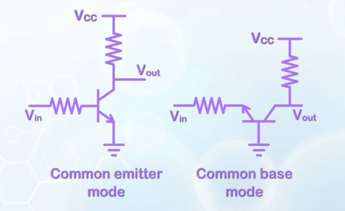
- In common base mode
- When a high voltage is applied to the emitter, the BJT is in cutoff mode, and no current flows
- When a negative voltage is applied, a current will flow through the load
- The maximum voltage the BJT can withstand is determined by the breakdown voltage of the reverse biased base-collector junction
- But the breakdown voltage also depends on the input, which can be high, low, or open
- In most cases, the worst case with lowest breakdown voltage is when the input is open
- This lowest breakdown voltage is denoted as
- In this case, the BJT just has the base-collector junction reverse biased, and the breakdown voltage is the same as that of a PN junction
- To increase breakdown voltage, the most effective way is to reduce doping on the lightly doped side (the collector side)
- In common emitter mode
- Again, the breakdown voltage is the lowest when the input is open
- The breakdown voltage is denoted as
- Assume the base-collector junction is reverse biased at a particular voltage such that for every 10 electrons entering the base-collector diode, there is a probability of generating one electron/hole pair
- Under normal condition, this voltage is not high enough to cause breakdown
- But in common-emitter configuration, the hole generated in the impact ionization process will enter the base
- As the base is open, the hole can only enter the emitter
- To allow the hole to enter the emitter, an associated voltage results at the floating base
- The ratio of the electron to hole current when the base emitter junction is lowered, is related to
- Assume
- These 100 electrons will enter the collector, causing 10 more electron/hole pairs to be generated
- This positive feedback will cause a very high collector current, even though the initial voltage is not high enough to cause breakdown
- To increase the breakdown voltage
- Reduce the chance to generate the first electron/hole pair by reducing the electric field, achievable by reducing the collector doping
- Reduce
- In common base mode
Summary of BJT Design
- Very high emitter doping relative to base, to increase
- Very small base width, to increase
- So that the BJT behaves more like an ideal switch with high gain
- Base width cannot be too small, limited by the Early effect and base punchthrough
- Collector doping should be low to reduce Early effect and increase breakdown voltage