About the physical structure of BJTs, and the switching transient behavior.
Physical BJT Design
On a physical wafer, BJTs can be placed horizontally or vertically. The latter is more common in integrated circuits, as doping is usually performed by ion implantation from the front side of the wafer, and it is easier to form heavily doped region near the surface.
- The emitter is usually placed on the top, followed by the base, and the lightly doped collector at the bottom
- The emitter can be directly connected from the top of the wafer
- The base must extend to the surface for external connection
- Similarly, the collector must also extend to the surface for external connection
- The collector resistance will be very high because it is lightly doped
- To reduce the resistance, a buried N+ layer is used, and an N+ region at the top of the collector region is formed during the emitter doping to provide an ohmic contact between the metal and the N- silicon collector
- Isolate BJT from other devices with a P region, usually the silicon substrate itself
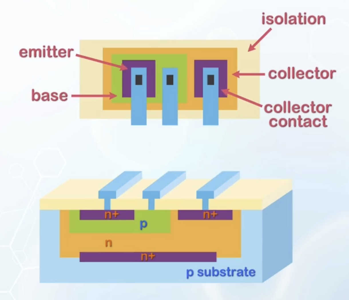
- The BJT only takes up a small area of the entire structure, and a large portion of area is used for device isolation and contacts
- Plot the doping concentration along the vertical cutline
- The curve:
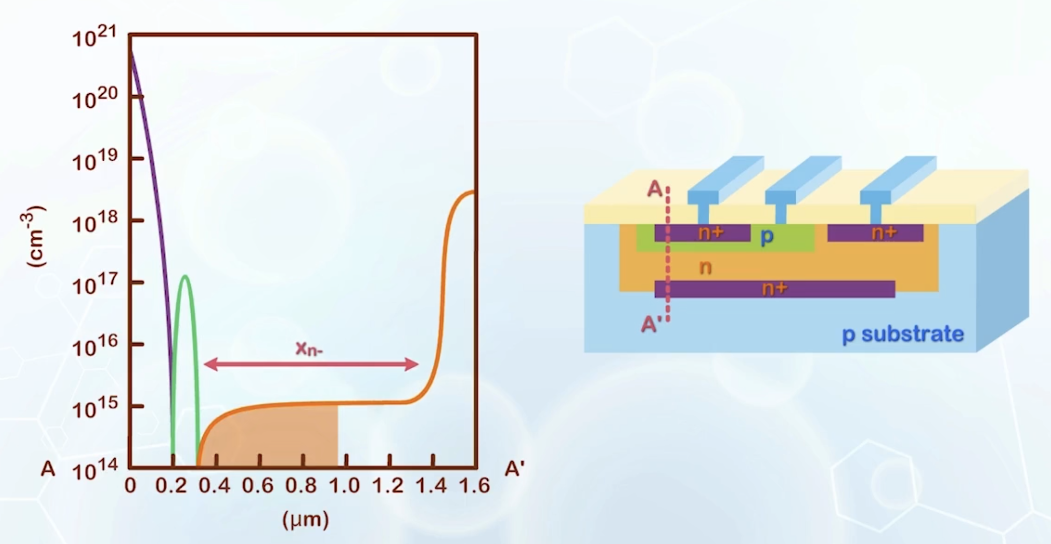
- The emitter is doped as heavily as possible (
- The base is narrow to reduce
- The collector is lightly doped to reduce the Early effect, to avoid base punchthrough, and to increase the breakdown voltage, usually limited by the fabrication process (
- The base doping should be selected carefully to trade off between
- At the end of the collector is the heavily doped N+ region to reduce collector resistance
- It is another trade off:
- When the reverse bias voltage of the base-collector junction is increased, the depletion region width
- If the N- region is too short, the depletion region will touch the N+ region before the maximum operation voltage, the depletion region will stop expanding, forcing the reverse voltage to drop across a smaller depletion width, increasing the electric field and reducing the breakdown voltage. The average effective doping in the depletion region also increases
- If the N- region is too long, electrons still have to travel a long distance in the lightly doped region, increasing the collector resistance
- When the reverse bias voltage of the base-collector junction is increased, the depletion region width
- It is another trade off:
- Besides the collector resistance, there is also a base resistance, and the holes need to travel a long distance to recombine with electrons in the emitter
- The resistance may be very high because the base is very thin
- To reduce the base resistance, the lateral dimension of the base should be kept small, to minimize the distance between the base contact and all locations at the base
- Adding another base contact to the left may also help, but that requires extra area
- In terms of layout, a long emitter is preferred to reduce the base resistance

- The curve:
Lateral BJT
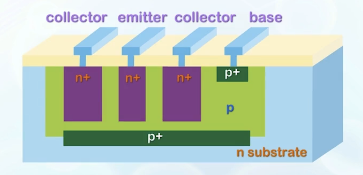
BJTs can also be laid out laterally on the wafer surface, as a lateral BJT.
- The region at the bottom of the structure must be P type, otherwise the N regions will be shorted without any barriers in between
- But if the substrate is P type, all the bases of lateral BJTs on the substrate will be shorted together
- Therefore, we have the P region forming the base extended to the region below the emitter and the collector, and build the whole device on an N substrate
- If breakdown voltage is not a concern, the collector can also be heavily doped to N+, and is formed together with the emitter, to simplify the fabrication process
- The separation between the emitter and the collector is kept small to reduce recombination at the base. This can be achieved by placing the base contact outside the main BJT structure
- Electrons can be injected to the base through the bottom of the N+ region. These electrons have to travel a much longer distance to reach the collector, and is easily lost to recombination
- Thus the base transport factor
- To improve the gain, the side wall area of the emitter should be increased relative to the bottom area, by making both the emitter and collector junctions deep, and the lateral dimension of the emitter small. An additional collector region can also be added to the other side of the emitter
- The depth of the base region is no longer restricted by the collector region, as in the vertical BJT, a P+ region can be introduced at the bottom of the base to reduce the base resistance
- Thus the base transport factor
The vertical dimension can be more precisely controlled relative to the lateral dimension in IC processing, the BJT technology is still dominated by vertical BJTs.
Turn on Transient
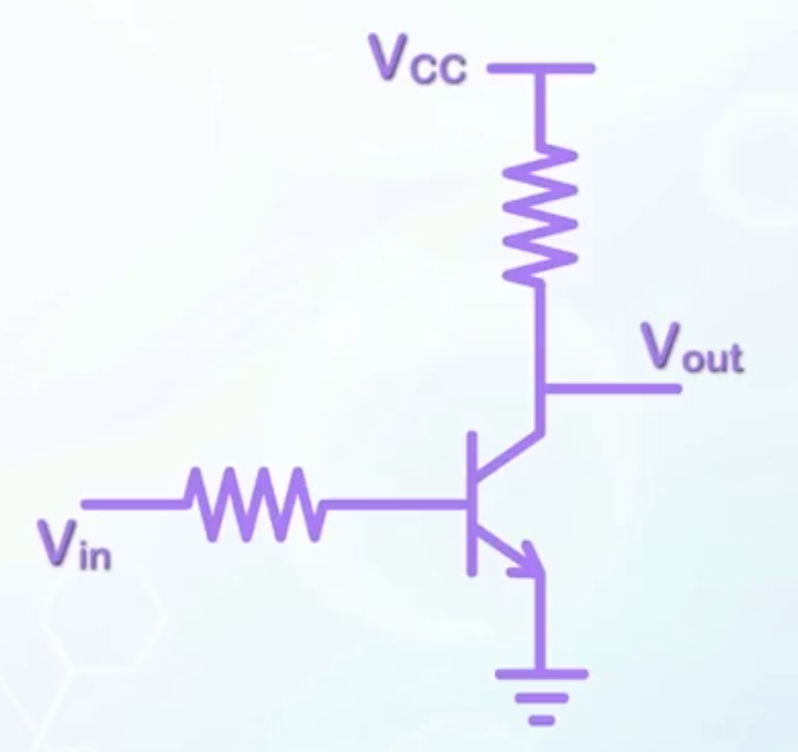
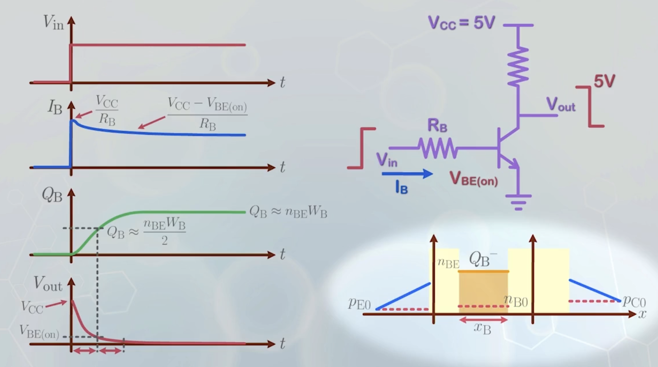
Consider BJT connected as an inverter.
- When a BJT is switched, it will switch between different operation modes, and has to be companied by the change in the amount of minority carrier charge
- Assume
- The BJT is behaving like an open-circuit,
- When the base voltage is switched to a logic high at time
- The initial base current is
Why VCC instead of Vin?
The logic high of
- Over a short period of time, the BJT will enter the forward active region
- The voltage across the base-emitter junction will be equal to
- All voltage beyond the value will be dropped across the resistor
- The voltage across the base-emitter junction will be equal to
- Now there are excess negatively charge electrons (the part below the minority carrier concentration distribution line) stored temporarily in the base region, and a base current is needed to supply holes to the base
- The amount of accumulated holes at the base
- Supplying electrons from the emitter is fast due to the large electron current
- Supplying holes from the base contact is slow due to the small base current
- Insufficient
- To calculate
- Over time,
- Assume
- The base current continues to supply the base charge
- The time at which the BTJ switches from forward active to saturation is marked in the timing diagram when the base charge is half of its saturation value
- At this point,
- The base current continues to supply the base charge
- The supply of the base charge is usually used as a measure for the speed of BJT switching
- The BJT is behaving like an open-circuit,
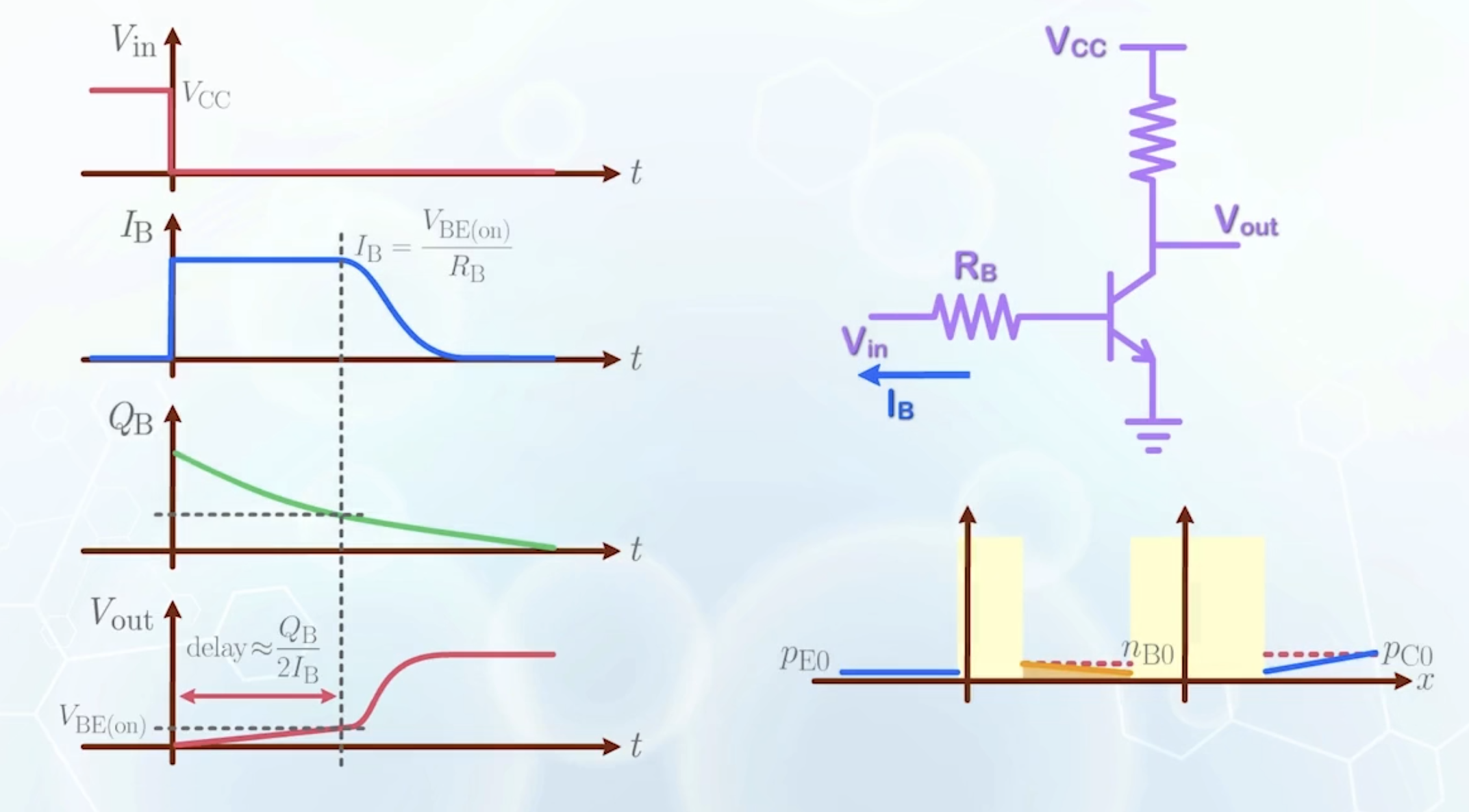
Turn off Transient
Similar to turn on, the delay for turn off is caused by the time to remove the accumulated base charge. It is actually more significant than the turn on delay.
- The charge at the base has to be removed before the BJT can enter forward active, then cutoff
- The removal of the accumulated holes is achieved by the base current passing through the base resistor to ground
- The minority carrier charge in the neutral base region near the base-emitter junction sustains the junction in forward bias, and junction voltage remains at
- The base current is given by
- The base current will remain constant for a long period of time, until the BJT enters forward active
- After that,
- There is a long delay before the output voltage rises
- The approximation delay to reach the forward active mode is given by
- The overall speed of a BJT when connected in the common-emitter configuration is usually limited by turn off
- The minority carrier charge in the neutral base region near the base-emitter junction sustains the junction in forward bias, and junction voltage remains at
Schottky BJT
Compared to switching from cutoff to forward active, switching from forward active to cutoff only increases the output voltage range by
By limiting the minimum voltage to
Due to the exponential dependence,
A Schottky diode can be connected between the base and collector to prevent the base-collector junction from going into deep saturation.
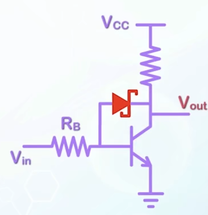
- When
- The turn on voltage for the Schottky diode is about
- When the BJT enters shallow saturation,
- The collector voltage will be maintained at
- The amount of base charge is kept about half of that without the Schottky diode
- The initial delay in turn off will be eliminated, and the overall switching speed is improved, and the trade off is the reduced output voltage swing
- To physically implement the Schottky diode, place a metal with Fermi level close to the valence band edge of Silicon at the base-collector junction
- It will form a Ohmic contact with the base, and a Schottky barrier with the collector
- Most commonly used metal for this structure is gold