About modeling BJTs under different operation modes, small signal model for amplifier design, frequency response and structural optimization.
The Ebers-Moll Model
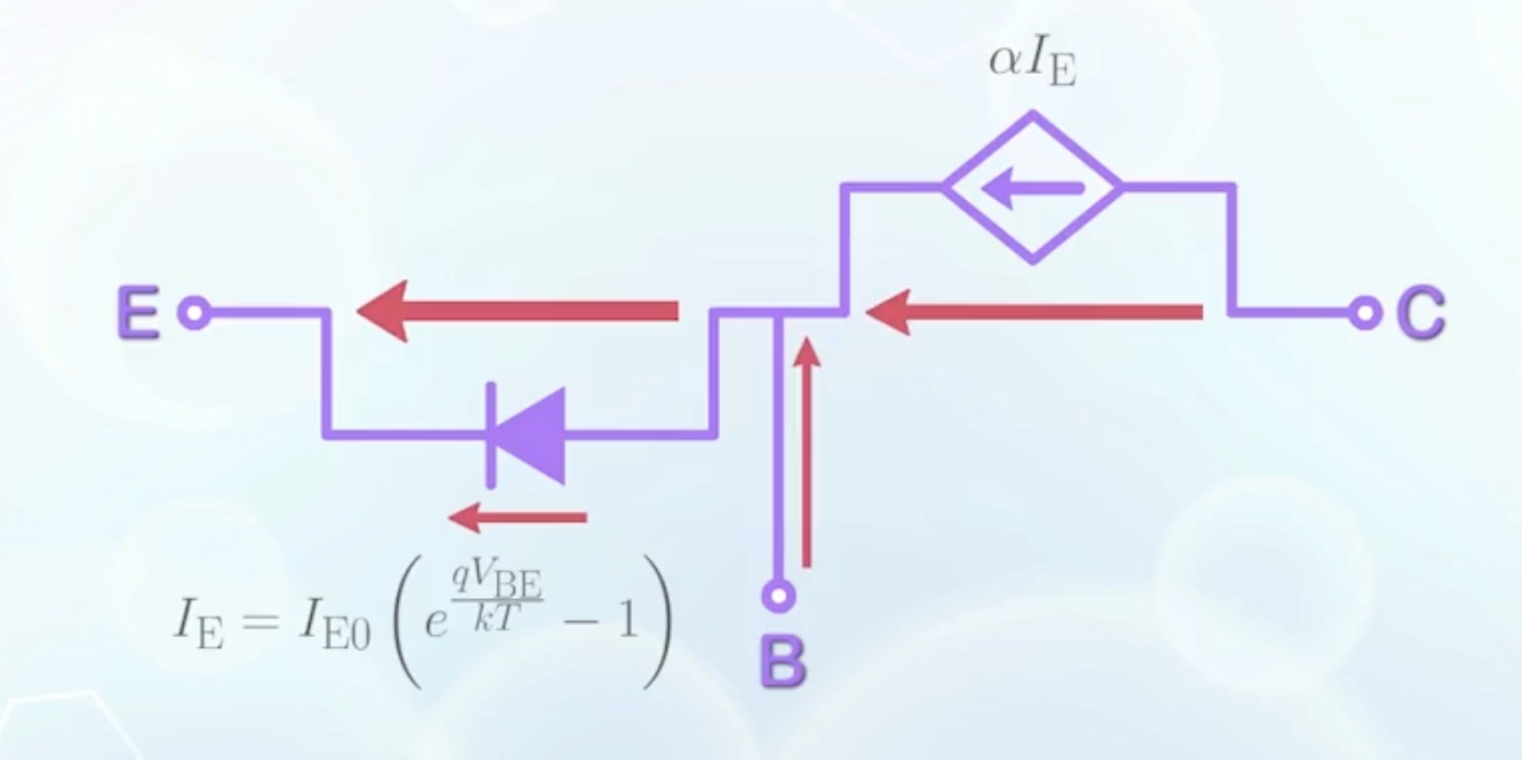
- To describe a BJT in forward active mode in steady state:
- The operation of a BJT is mainly based on the PN junction diode between the base and emitter, we place a diode between the base and emitter in the model
- The emitter current is just the diode current given by
- A current controlled current source is placed between the collector and emitter, to represent
- The difference between
- The model describes exactly the BJT operation in forward active mode in steady state
- In reverse active mode:
- The transistor actions come from the base-collector junction, which is another PN junction diode
- The collector current is again given by the ideal diode equation
- A current controlled current source is placed between the emitter and collector, to represent
- The
- To distinguish the two, we denote the reverse active mode one as
- The
- The model for BJT under reverse active mode:
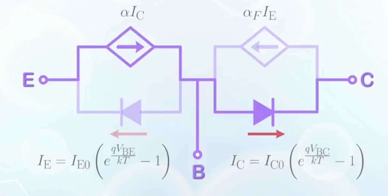
- In forward active mode, the base-collector diode is in reverse bias, and can be regarded as an open circuit,
- The same applies to reverse active mode, where the forward-active-mode-related components can be ignored
- In cutoff mode, all diodes are considered as open circuits, and no current flows
- In saturation mode, both diodes are forward biased, and injects current to the base
- The net current is determined by the relative magnitudes of the injection currents
- The model now can describe the BJT operation in all four modes
- It should be noted that the diodes in the model only represent the function of the voltage-controlled current source in the diode model
- To capture the dynamic behavior, the full model of the diode, as discussed in the PN junction section should be included
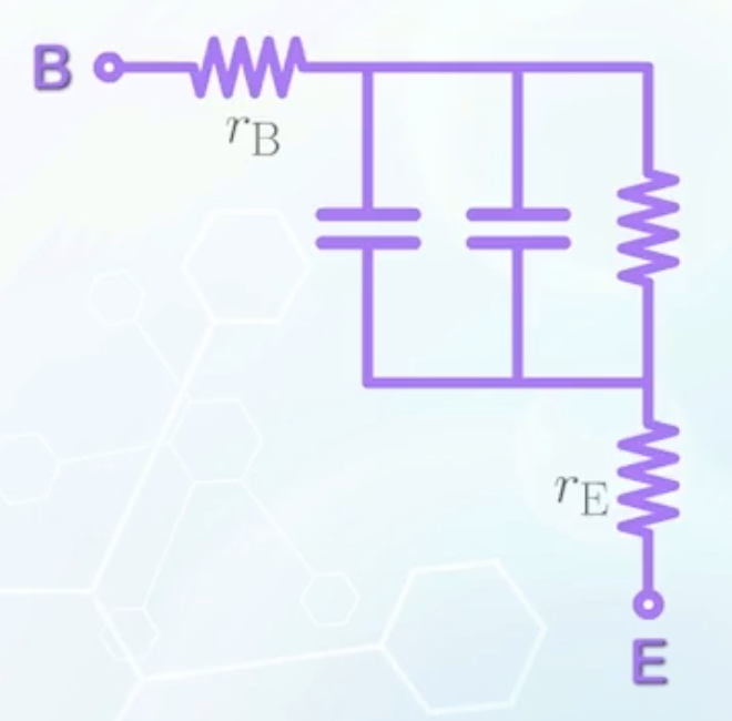
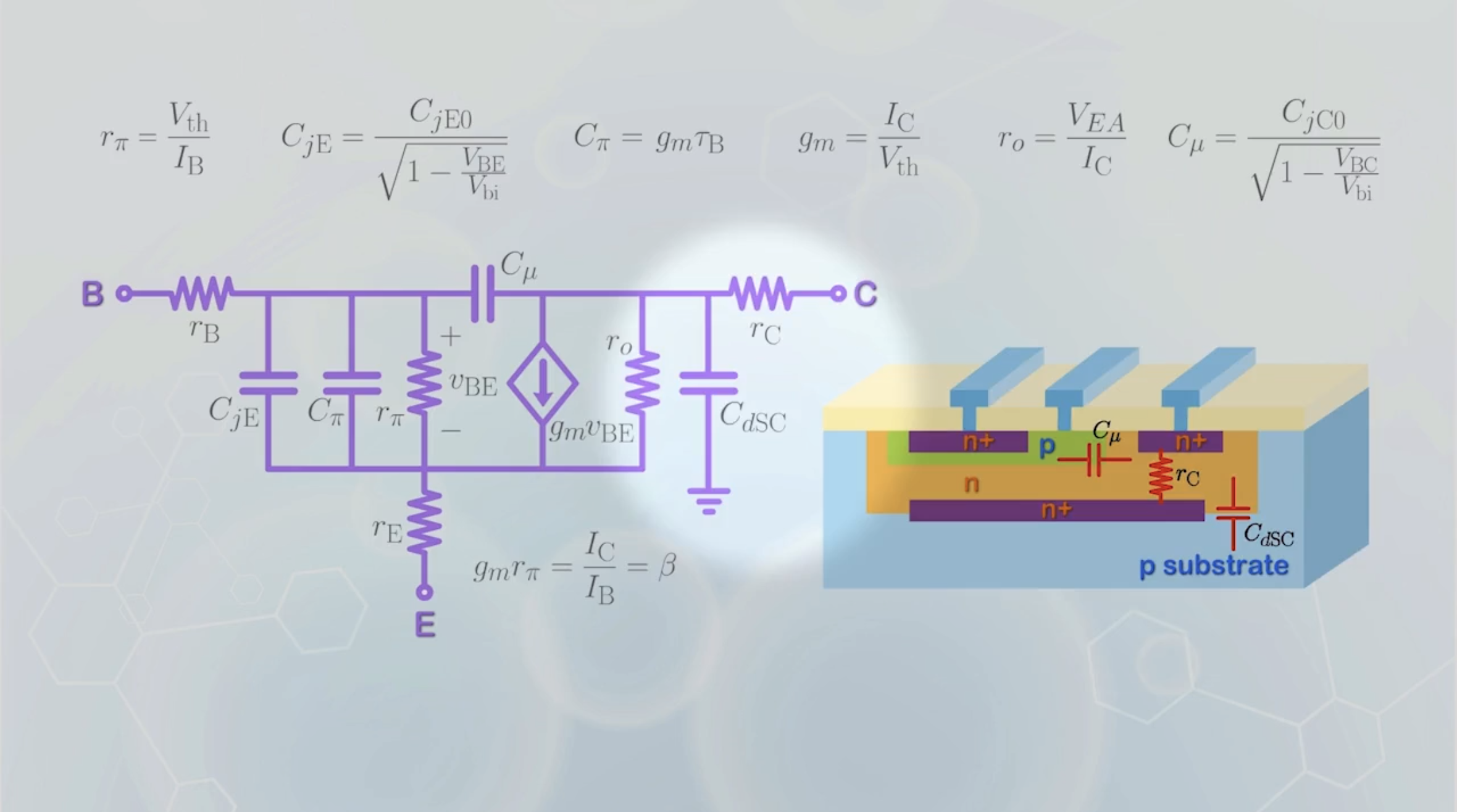
- The currents though the base, emitter and the collector terminals are different in the case of BJT, the base, emitter and collector resistances have to be associated with the respective terminals
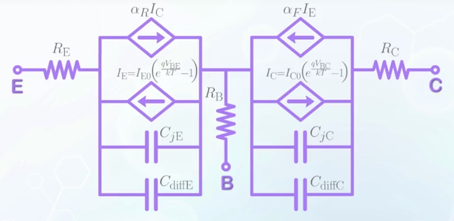
- This is still an over-simplified situation, as it assumes the diodes operate independently
- More detailed models should be able to capture the interaction between the two junctions
The Small Signal Model
Besides digital switches, BJTs can also be used as amplifiers, common in signal processing circuits.
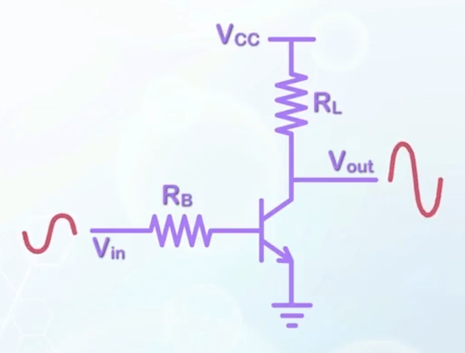
- A very small varying voltage can be applied to the input
- Based on the exponential relationship between
- The collector current change will be converted to the output voltage, multiplied by the load resistance
- The input signal is assumed to be small, or it will saturate the waveform, leading to clipping
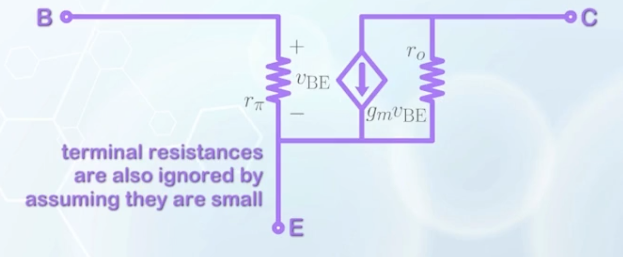
- For a very small signal input, we can linearize the circuit around a particular biasing point, usually in the forward active mode
- To construct the small signal model
- Start from the PN junction between the base and emitter
- Copy the small signal diode model from the PN junction section
- With the emitter assumed to be grounded, the resistance
- In BJT, we prefer to express
- Physically,
- Now back to
- The value
- Transconductance represents the slope of the linearized characteristics of BJT:
- In BJT, we prefer to express
- Copy the small signal diode model from the PN junction section
- Between the collector and the emitter, the current is controlled by the signal at the base-emitter junction
- It can be represented by a current controlled current source
- Or with a voltage controlled current source
- It should be noted that
- In addition to the current source, that gives the collector current, the Early effect contributes a resistor
- It can be represented by a current controlled current source
- Between the base and collector, there is a reverse bias junction capacitance
- It is the depletion capacitance between the base-collector junction
- It is the depletion capacitance between the base-collector junction
- There is another series resistance for the collector
- The collector is surrounded by a P substrate for isolation, introducing a reverse bias junction capacitance
- Start from the PN junction between the base and emitter
Frequency Response
For a transistor used as an amplifier, the output can follow input when the input frequency is low enough. In such case, the capacitors in the small signal model can be considered as open circuits, and removed from the model. The gain of the transistor becomes constant.
When frequency increases, it is possible that before a carrier can reach the collector, the signal has already been reversed. In such case, the collector current does not respond to the change of the input signal.
The gain of the amplifier drops when the input frequency becomes higher than a certain value, due to the capacitance, limiting the frequency range a BJT can function properly.
- The speed of a BJT, in terms of the highest frequency it can handle, is usually characterized by the transit frequency
- In the
- The drop in beta is linear with the log of frequency
- Extending the linear drop line to the frequency at which
- At
- Skipping the math details, the final result is
- We care about how
- At very small
- When
- The maximum
- With
- Further increasing
Structural Optimization
Compared to MOSFET, BJTs are more commonly used to make discrete devices instead of integrated circuits.
The advantages of BJTs include
- High current drive capability
- Sustains high voltage
However, we usually have either NPN or PNP BJTs, but not both, on a single wafer, compared to the complementary MOSFET pairs. Possible complementary BJT structures are complex and not a popular choice.
To improve the performance of a BJT circuit, it is important to reduce the parasitic elements.
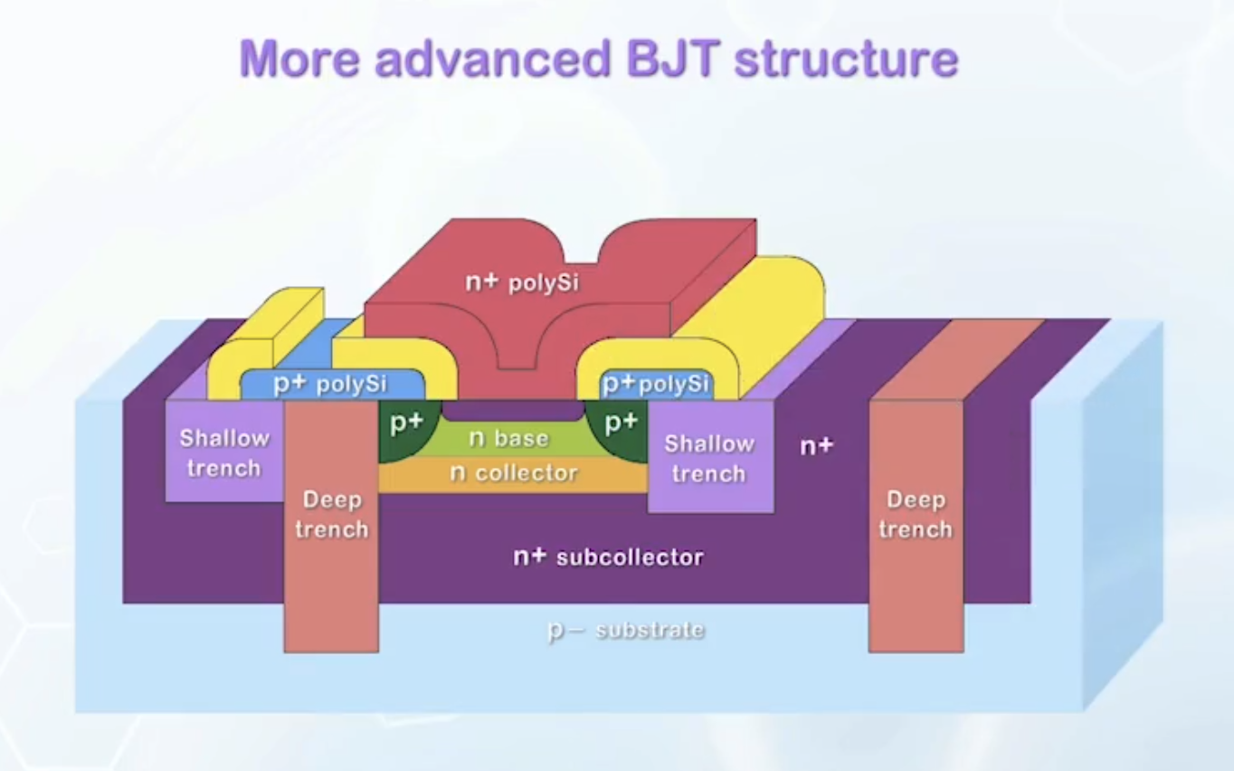
- The emitter is extended by adding an N+ polysilicon layer, giving a long emitter length to reduce the diffusion hole current from the base to the emitter
- A P+ region is added to the base outside the transistor region to reduce the base resistance
- The P+ polysilicon layer is used to contact the P+ base, to avoid including contact that consumes large area in the transistor structure
- Trench isolation filled with insulator is used to isolate different regions instead of just a reverse junction, to avoid the parasitic junction capacitance
Congratulations!
We have reached the end of Principle of Semiconductor Devices Part I: Semiconductors, PN Junctions and Bipolar Junction Transistors 🎉
But… Part II awaits! 😨 More stuff needs to be learnt…
But for now, take a break and celebrate your achievement! 🥳