About density of states, Fermi-Dirac distribution, carrier density calculation, effective density of states, Boltzmann approximation, and water analogy for the bandgap.
- The density of carriers in a solid semiconductor depends on three factors:
- density of state available in an energy band
- size of band gap
- temperature of the operation environment
Density of States
- State: a space to hold one electron, becomes a hole without an electron.
- Density of states are not uniformly distributed in an energy band.
- Fewer states closer to the band gap
- More states further away from the band gap
- Exact value of
- Exact value of
Fermi-Dirac Distribution
- Without energy supplied (absolute zero temperature), all electrons stay at lowest energy states.
- With energy supplied:
- The distribution of carriers in the states of a band is governed by the Fermi-Dirac distribution function:
- The distribution of carriers in the states of a band is governed by the Fermi-Dirac distribution function:
More on Fermi-Dirac Distribution
When
It is an abrupt function.
When
Thus,
- Materials with a band gap:
- In the valence band: the probability of holes occupying a state
Calculating Carrier Density
- Total number:
- For pure or intrinsic silicon,
- For pure or intrinsic silicon,
Equivalent (Effective) Density of States
- We do not care about
- Simplify:
- Assume energy band is narrow, all states are at
- Define an equivalent density of states
- Then:
- Assume energy band is narrow, all states are at
- For silicon at room temperature (
Boltzmann Approximation
- Thus,
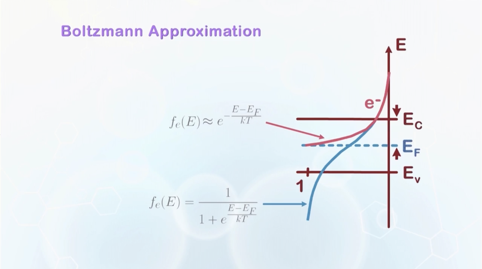
- After the approximation,
- Finally, the intrinsic electron concentration and the intrinsic hole concentration:
- Multiplying the two equations:
- Number of carriers of silicon at room temperature:
Water Analogy for the bandgap
- A light, hollow, closed box partially filled with water.
- At the water to air interface, the probability to find a water molecule is
- Uniform external potential -> placing the box in a larger water tank where the water level represents the external potential.
- The box will float, aligning the water level inside the box with the water level outside -> The Fermi level is a reference energy level with respect to the surrounding.
- The band gap is a solid box without water molecules dropped inside the box, it will float in water, and the plane separating the floating part and sinking part is the Fermi level.
- The solid box has cracks, water molecules can jump above through the box through the cracks -> electrons excited from valence band to conduction band.
- External voltage applied -> external water level changes -> Fermi level at the two ends of the semiconductor changes -> current flows.
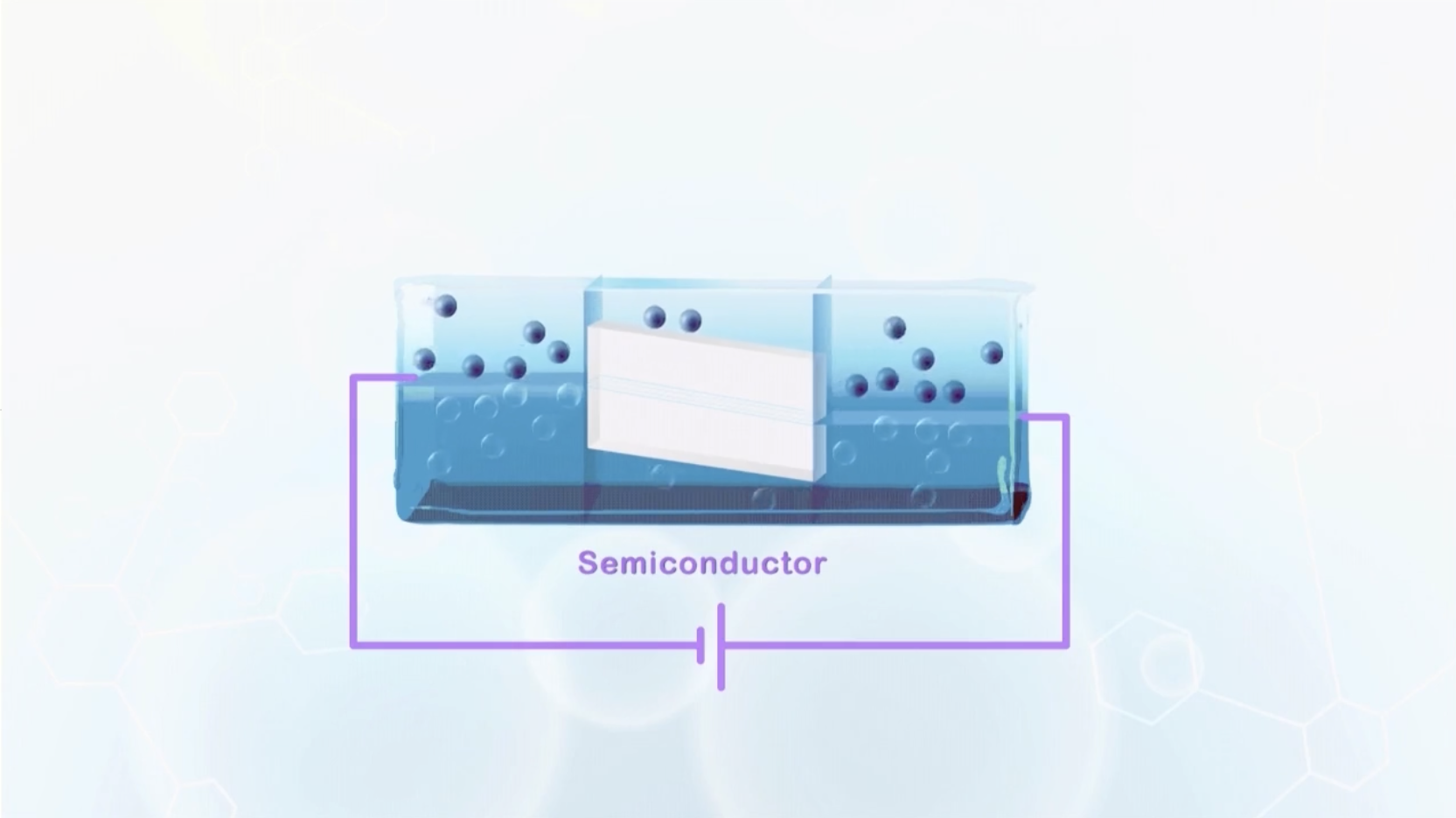
- Battery only controls the two ends, inside the semiconductor, the Fermi level is subject to the properties of the material.