About carrier statistics with respect to locations, external voltages, and the diffusion current with applied voltage.
Carrier Statistics with Respect to Locations
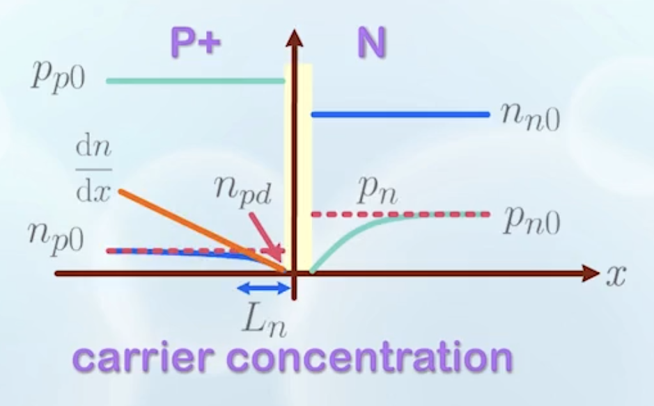
- In a P+/N junction:
- Carrier concentration
- Denotations:
- We draw the graph in log scale as carrier concentration varies a lot
- Carrier concentration
- Carrier concentration in the depletion region is not a constant, but varies with location
- It is difficult to calculate, so we simply ignore it, assuming it is very small compared to the neutral regions
Carrier Motion at Thermal Equilibrium
Discussing only electrons
We will only be discussing electrons from now on, but the discussion applies to holes as well.
- No net current flow at thermal equilibrium, but carriers are not stationary
- In the conduction band
- On the N side, higher electron concentration pushes electrons to diffuse to the P side
- Some of the electrons are driven back by drift
- There are many electrons on the N side, but most with energy lower than
- Electrons that can move freely across the two sides are those with energy higher than
- On the P side, concentration of these high-energy electrons are
- On the N side, concentration of electrons is governed by the Fermi-Dirac distribution, where
Fermi-Level Under External Voltage
- The PN junction symbol

- Positive Bias/Forward Bias: Positive voltage
- Negative Bias/Reverse Bias: Negative voltage
- At reverse bias, alignment of the Fermi levels on the two sides is broken
- Fermi level on the P side is raised by
- Fermi level is the same across the neutral regions, but there is a discontinuity across the depletion region
- In the depletion region, there are externally injected carriers, so the equilibrium cannot be assumed. Simple Fermi-Dirac distribution with one Fermi level does not apply
- Must be handled with some advanced concepts of quasi-Fermi levels
- For now, we will ignore the depletion region and focus on the neutral regions
- Fermi level on the P side is raised by
Energy Band Bending Under Reverse Bias
- When a reverse bias is applied, we need to find the new barrier height and the new depletion region width
- For the barrier height:
- At thermal equilibrium, the barrier height is
- Under reverse bias, the barrier height is raised by
- New barrier height:
Why negative?
- At thermal equilibrium, the barrier height is
- For the depletion region width:
- Charge neutrality still holds
- The second equation becomes
- Solving the two equations, we get
- Assuming
- Charge neutrality still holds
Carrier Concentration at Reverse Bias
- When an electron enters the edge of the depletion region from the P side, it moves to the N side due to the slope in the band diagram (caused mainly by drift)
- Electron concentration at the edge of the depletion region on the P side is lower
- More electrons from the rest of the P side diffuse to the edge of the depletion region
- When we draw the graph of carrier concentration
- The concentration on the P side becomes lower as
- The concentration on the N side remains the same (
- Similarly for holes, the concentration on the N side becomes lower as
- The concentration on the P side becomes lower as
Diffusion Current Under Reverse Bias
- Current calculation is achieved by counting the number of electrons crossing a particular location per unit time
- It is much easier to do so at locations with lower carrier concentration
- For electrons, we calculate the current on the P side near the edge of the depletion region
- The driving force is mainly diffusion
- Current density for electrons (current per unit area):
- When
- When
- The corresponding current for holes is
- The negative sign is because holes move in the opposite direction to electrons
- In the graph,
 It represents the average distance an electron can diffuse before recombining. We can assume it is a known constant at this stage.
- With these two notations, we have
Reverse Bias Current of a PN Junction
- A few more assumptions:
- The carrier statistics in the neutral N region is not affected by the bias voltage, as the number of electrons added is very small compared to the number of electrons already there
- The depletion region is very small compared to the neutral regions, so we can ignore its thickness
- With these assumptions,
- This is because concentration cannot change abruptly from P side to N side, as we’ve ignored the depletion region thickness
- Calculate carrier concentration with Fermi-Dirac distribution
- Finally,
- The same for holes:
- Combine the two:
Conditions Under Forward Bias…
- Everything is the same as reverse bias, except that
- When
- We can denote
- The final equation is