About non-ideal PN junction characteristics, PN junction turn-on, breakdown, temperature effects, and how to design a PN junction.
Ideal Diode Current in Log Scale
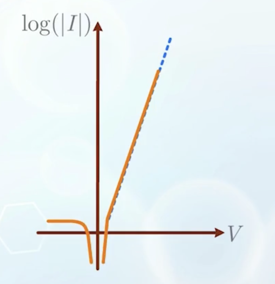
- When
- When
- The slope of the linear region can indicate how abruptly we can turn on the diode with applied voltage
- The unit of slope in log scale is a bit difficult to express, so we tend to refer
- Once
A Very Important Reference
At room temperature:
- This means that for every increase of
- Remember this value
- A smaller swing means a steeper slope, which means the diode can be turned on more abruptly with a smaller change in voltage
- This means that for every increase of
- Or
- The thermal voltage
- With the same unit as voltage
- Or
Recombination Current in the Depletion Region
- The characteristics of a real diode differs from the real one
- At low current, measured current is usually higher than the ideal one
- When
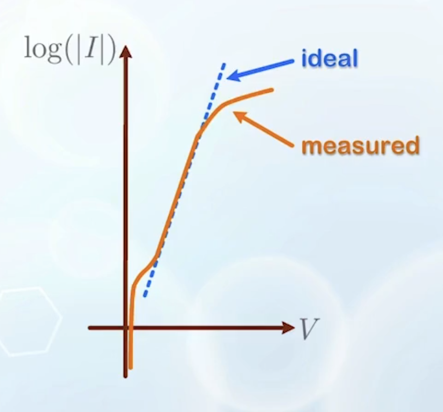
- The ideal equation assumes no recombination happens in the depletion region
- However, in reality, recombinations happen in the depletion region
- As discussed in the previous chapter, recombination is a mechanism that encourages a higher current flow
- Therefore, recombination in the depletion region leads to higher majority carrier current
- This current can be ignored when
- When
- This current can be ignored when
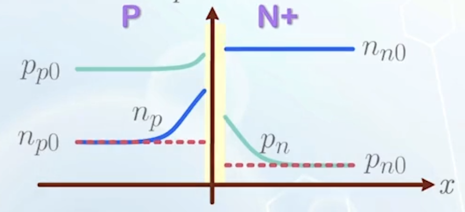
High Level Injection
- The ideal equation assumes the number of injected minority carriers does not effect the majority carrier concentration
- However, when
- On the P side:
- Electrons are injected from the N side
- High level electron injection causes accumulation of negative charges
- This accumulation of negative charges repels holes, causing holes to accumulate on the P side near the depletion region
- This creates a diffusion force which drives holes away against its motion in the ideal forward bias case
- This is the high-level injection effect
- The accumulation of holes is insignificant when
- But can be very significant when
- The high-level injection effect always takes place first at the lightly doped side (because the majority carrier concentration is lower)
Complete PN Junction Turn-on
- When we further increase
- As discussed in Chapter 1.5, the diode now behaves like a resistor
- Gives a straight line in linear scale
- Shows saturating behavior in log scale
- When you see the current increases with voltage, the diode is most likely to be in the resistive region already
- So the ideal diode equation is only valid for the
- So the ideal diode equation is only valid for the
- Fully turn-on region: the resistive region when the depletion region disappears
- Turn-on voltage
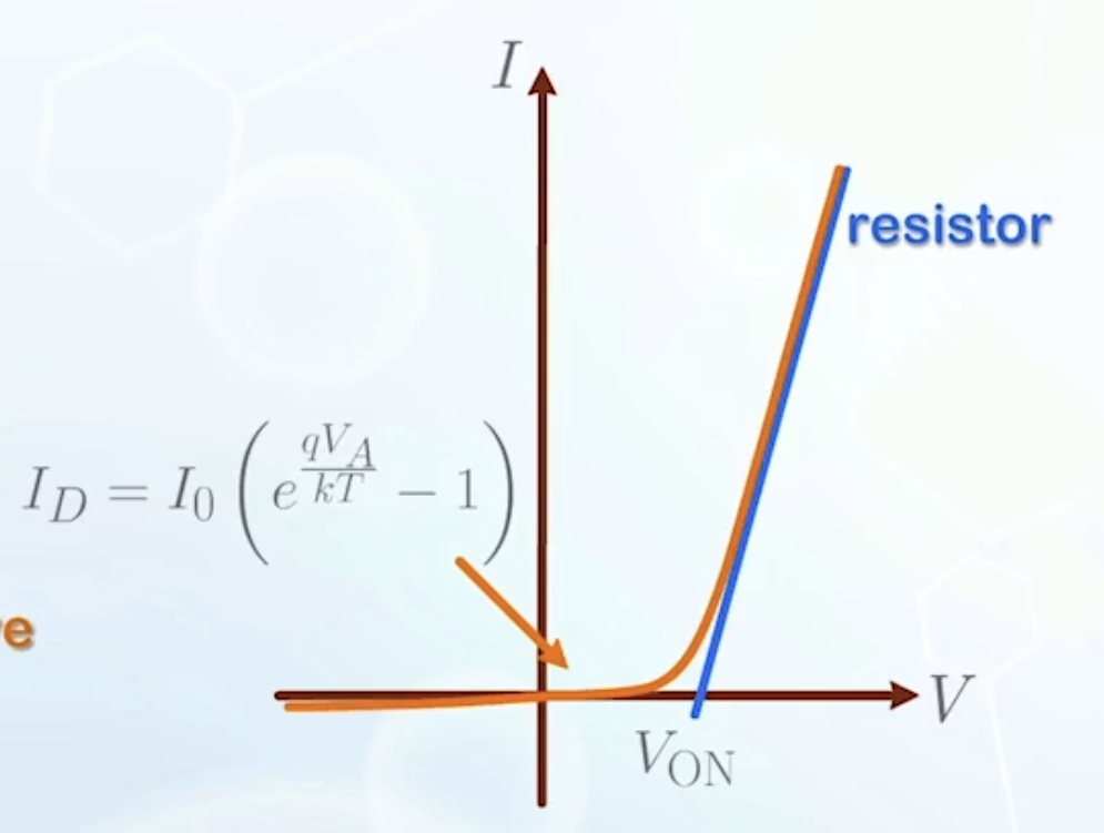
- The turn-on voltage for a silicon diode is assumed to be around
PN Junction Breakdown
- The ideal equation shows that the current remains small for any negative
- However, in reality, when
- This is called reverse breakdown
- Two different mechanisms can cause reverse breakdown
- Avalanche breakdown
- A high electric field is created in the depletion region when
- This high electric field can accelerate carriers to very high speeds
- These high-speed carriers can collide with atoms in the crystal lattice and generate electron-hole pairs
- When the reverse bias is high enough, the additional electron-hole pairs, together with the original carriers, can create more collisions and generate even more electron-hole pairs, resulting in a large reverse current
- It is like a avalanche caused by a small snowball
- A high electric field is created in the depletion region when
- Zener breakdown
- Recall the equation used to calculate the depletion region width:
- When the doping concentration is very high, the depletion region width can be very small
- For a narrow junction with high reverse bias voltage, the lateral separation between the conduction band and the valence band can be very small
- This allows electrons in the valence band to tunnel through the energy barrier to the conduction
- This tunneling effect can create a large reverse current
- Recall the equation used to calculate the depletion region width:
- Avalanche breakdown
- Breakdown may not be destructive
- If the current is limited, the diode can recover after the reverse bias is removed
- What really destroys the diode is the heat generated by the large current, melting the junction
Temperature Effects
- At high temperature, the impact of carriers added by doping is less significant
- Both sides of the junction behave more like intrinsic semiconductors
- The junction will be less effective as a rectifier, more like a resistor
- The slope of the ideal region decreases, leading to a larger swing
- Rectifying properties are degraded
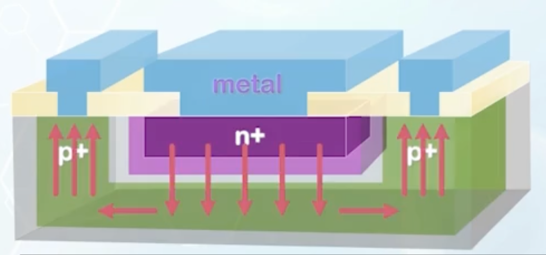
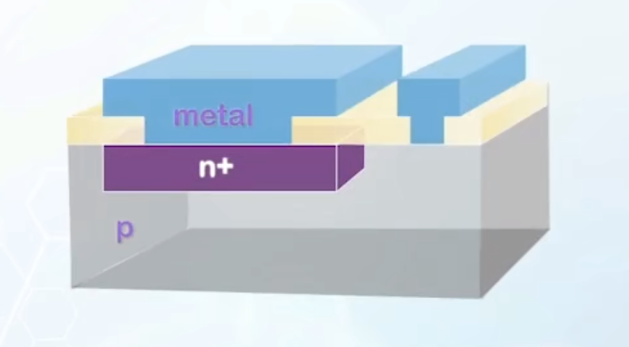
PN Junction Design
- The current follows a more complicated 2D or 3D pattern
- For the heavily doped side, the resistance is relatively low and close to ideal, it can be doped as heavily as possible, subjective to the solid solubility limit
- The lightly doped side controls the properties of the diode
- If we simply connect metal to the lightly doped side, the series resistance will be very high
- The metal-semiconductor contact resistance is usually very high
- And the current may concentrate on a small area, due to the non-uniform resistance distribution
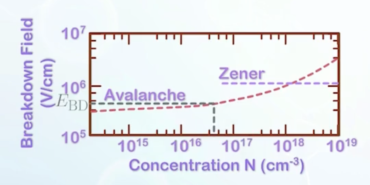
- We wish to decrease the resistance by adopting a higher doping concentration, but this may significantly decrease the breakdown voltage
- Design goal: select a high enough doping concentration to reduce the series resistance, while maintaining a high enough breakdown voltage
- The breakdown condition is related to the maximum electric field in the depletion region
- The avalanche breakdown voltage can be plotted against the doping concentration on the lightly doped side
- Once the doping concentration passes a certain value, the Zener breakdown will take over
- Once the electric field/slope of the band is known, the lateral separation between the conduction band and the valence band (tunneling distance) can be calculated
- It is important to understand how the electric field changes with doping concentration
- Recall how we calculate the depletion region width
- According to Gauss’s law, the electric field in the depletion region is
- Now we have
- Now we have the relationship between the maximum electric field and the doping concentration
- To choose a proper doping concentration, we begin with an arbitrary concentration
- Then we can calculate
- We compare
- If
- Else, we need to reduce the doping concentration and repeat the process
- As an engineer, make sure to leave enough margin
- Besides the depletion region, a diode also consists of neutral regions
- The neutral regions contribute little to the rectifying properties of the diode, but contribute to the series resistance
- We can increase the doping concentration to reduce the resistance
- We can also add another P contact to make the resistance more uniform at different locations