About the charge storage effects, PN junction diode models, and parameter extraction.
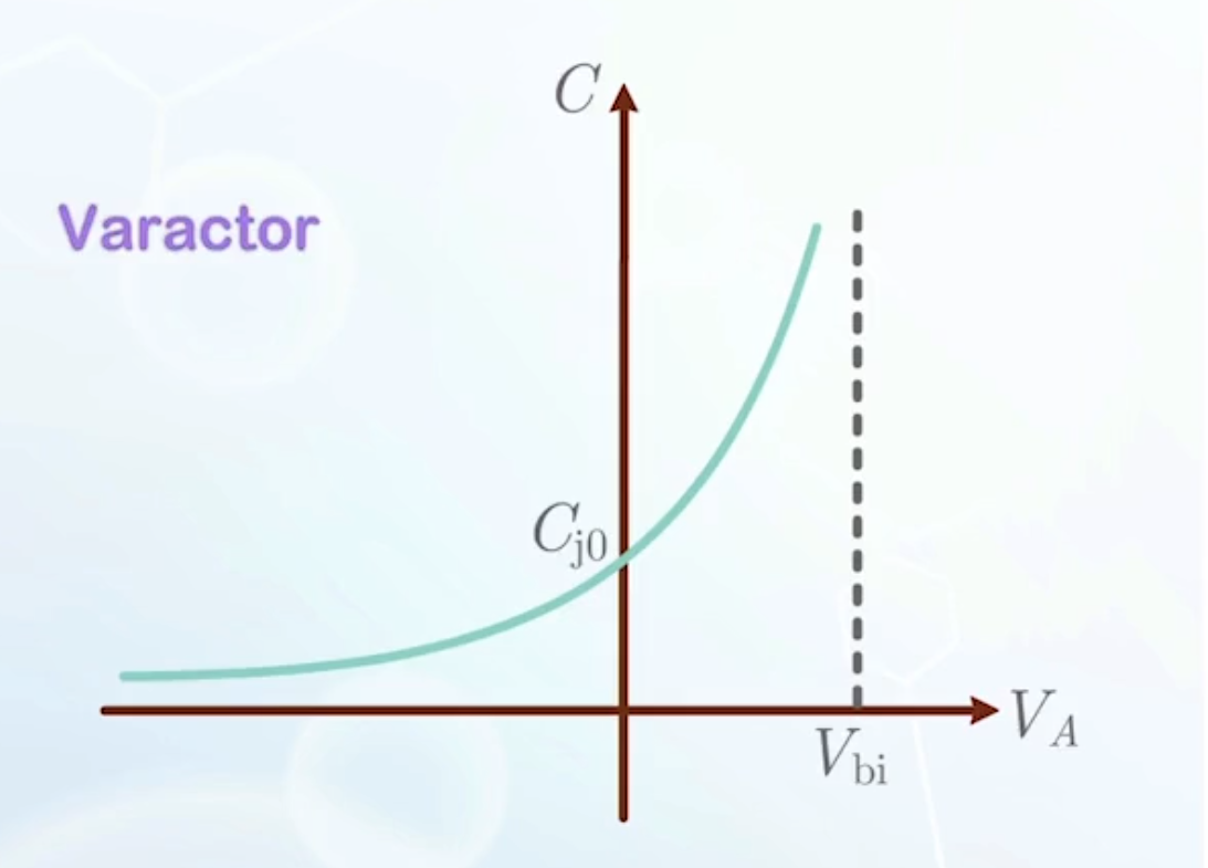
Reverse Bias Junction Capacitance
- When switching a diode with time varying voltage, response may be delayed
- Charges need to be accumulated to reach steady state
- The delay can be modeled as a capacitance within the diode
- Under reverse bias, the diode can be modeled as an insulator sandwiched between two conductors, or a parallel-plate capacitor
- The depletion region is the insulator
- The P and N regions are the conductors
- Its capacitance is denoted as
- We normalize it with respect to area so we can drop
- Substituting
- The function shows that
- Lower doping concentration leads to lower junction capacitance, due to wider depletion region
- Capacitance of a diode can be changed by applying different voltages, making it a varactor (variable capacitor), which can select a signal at a specific frequency, but rejecting others.
Forward Bias Diffusion Capacitance
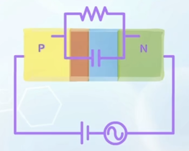
- Under forward bias, a current conduction path is established
- The parallel-plate capacitor model is no longer valid
- The diode can be modeled as a resistor in parallel with a capacitor
- For non-linear capacitors (as the case here), capacitance is defined as
- A PN junction under forward bias stores two kinds of charge
- The charges in the depletion region, which has already been modeled as
- The charges of excess minority carriers injected from the opposite sides, temporarily stored before leaving (small under reverse bias, so we ignored it)
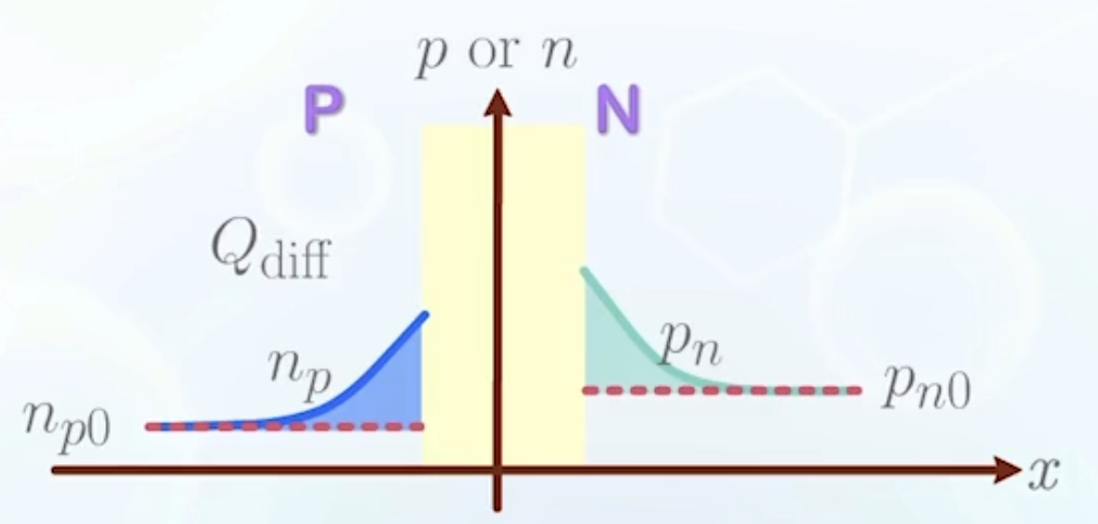
- Carrier concentration at thermal equilibrium is not counted as stored charge since the system is electrically neutral
- The excess minority carrier charge (diffusion charge) in P side is
- Assuming injected carriers
- Assuming injected carriers
- Adding the contribution from N side, we have the total diffusion charge
- Differentiating it with respect to
- The charges in the depletion region, which has already been modeled as
Large Signal PN Junction Model
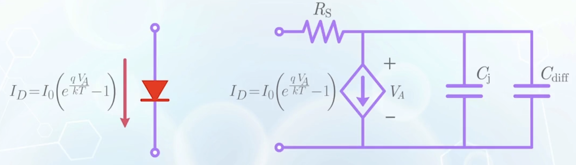
- The ideal PN junction current-voltage relationship is
- The neutral regions can be represented as resistor
- To account for the charge storage effects, we add two capacitors in parallel
Small Signal PN Junction Model
When PN junction can only be operated over a small region around a bias voltage
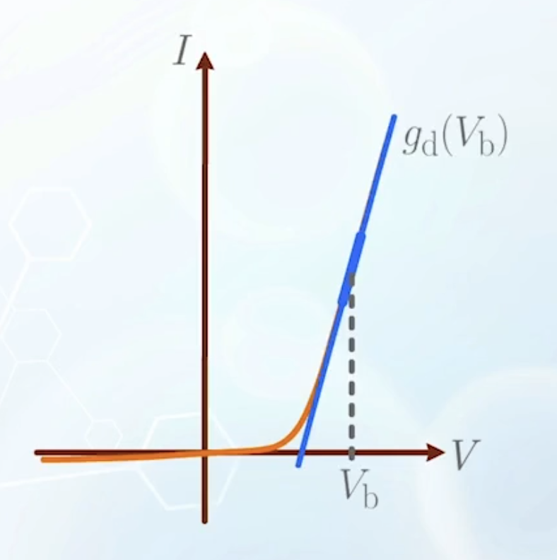
- The
- The voltage-controlled source can be replaced with a resistor whose conductance is
- All other components (
PN Junction Diode Parameter Extraction
A sample data sheet provided by diode manufacturer:
CHARACTERISTICS
| SYM. | PARAMETER | CONDITIONS | MAX. | UNIT |
|---|---|---|---|---|
| forward voltage | 1 | |||
| reverse current | 100 | |||
| diode capacitance | 2 | |||
| reverse breakdown voltage | 300 | |||
| series resistance | 3 | |||
| ideality factor | 1.05 | |||
| reverse recovery time | when switched from | 50 |
These values are mesured instead of calculated, and the process is called parameter extraction.
It is the process to find the values of these unknown parameters so that the values predicted by the model give the best fit to the experimental data
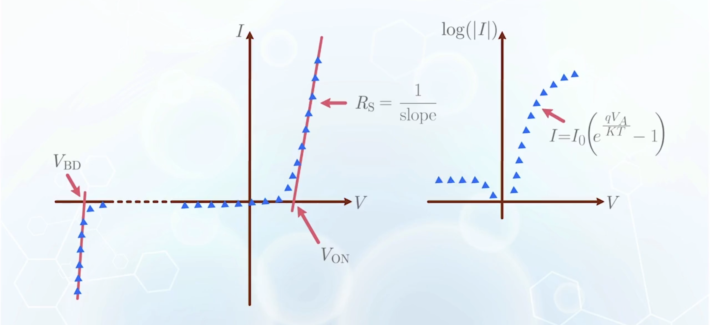
- In the forward bias region, before the diode fully turns on, the ideal diode equation may not match the experimental data, due to non-ideal effects
- The ideality factor
- The modified ideal diode equation is
- For an ideal diode,
- The ideality factor