About the optical properties of PN junctions, how to apply them to photo detectors, solar cells, and LEDs, and how to design these devices for better performance.
Optical Properties of Semiconductors
- Electron-hole pairs will be generated when energy is supplied
- The energy can come from thermal energy
- But can also come from light (particles called photons)
- The energy is related to its wavelength
- With given units:
- If the photon energy is higher than the bandgap energy, it will be absorbed and excite an electron from valance band to conduction band
- If the photon energy is lower than the bandgap energy, it will not be absorbed, but transmitted through the material
- Explains why transparent materials are usually insulators with large bandgap
- Wavelength of visible light is from
- Silicon absorbs light from infrared to the entire visible spectrum
- When electron-hole pairs are generated by light absorption, generated carriers tend to move together by diffusion, so the net current is 0. They will eventually recombine in a region without light
- But if light is shining on the depletion region of a PN junction, the electric field will cause electrons and holes to move in opposite directions, leading to a current when both sides of junction are shorted, having the same voltage
- The short-circuit current
- The current flows from N side to P side, so it is negative according to the convention of PN junction diode current equation
- With bias voltage applied, the total current is the sum of bias-induced PN junction current and the photo-induced optical current:
- In the I-V curve:
- At higher light density, the curve shifts downwards
- The curve cuts the
- Happens when the reverse
- Happens when the reverse
- The short-circuit current
Photo Detectors
- A simple photo detector circuit
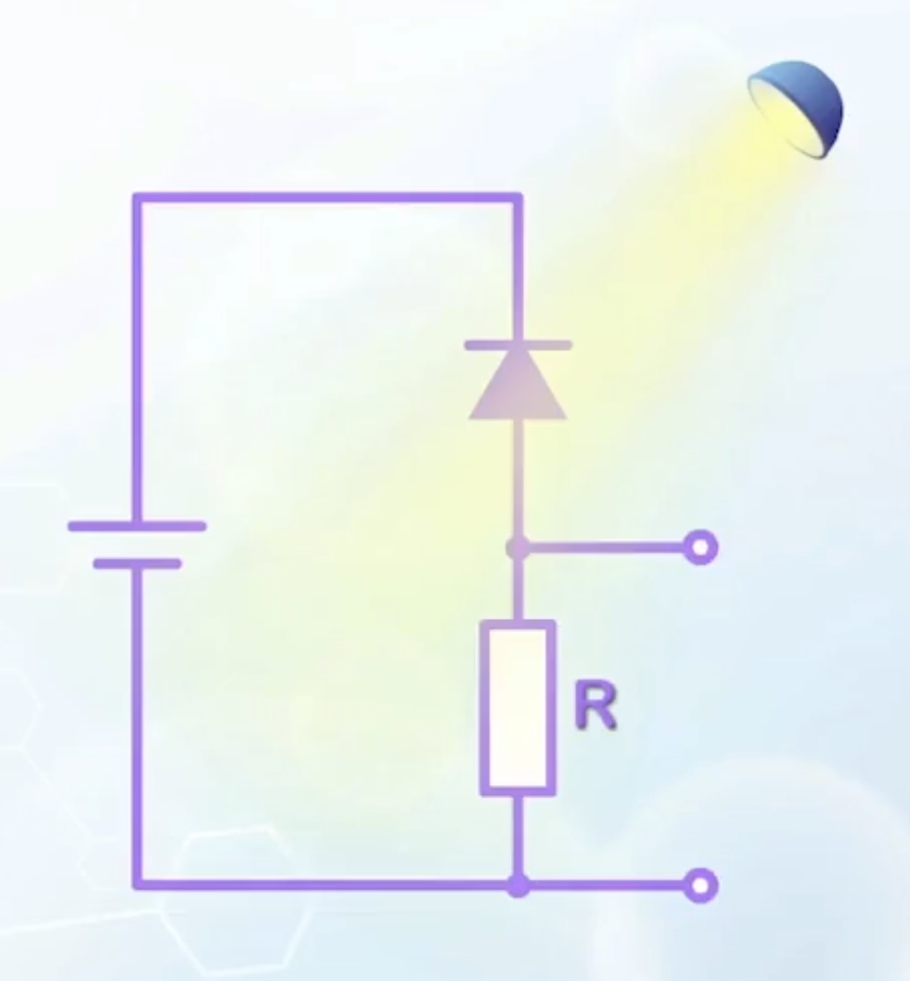
- A reverse bias is applied, and the diode current is equal to
- Without light, the output voltage is
- With light, the output voltage is:
- A reverse bias is applied, and the diode current is equal to
Solar Cells
- In a photo detector circuit, the PN junction is forced to work in reverse bias mode, or the 3rd quadrant of the I-V curve, where power is consumed (like a resistor)
- The current flows from P side to N side, following the voltage polarity
- In a solar cell, a current is generated to flow from the N side terminal to the P side terminal
- The current is fed to the resistor and generates a forward bias within the diode
- The diode now works in the 4th quadrant of the I-V characteristic, where the direction of current flow is opposite to the voltage polarity
- Converts optical energy to electrical energy, is a solar cell
- The operation point of the circuit is determined by the I-V curve of the diode, and the resistor load
- Define P -> N to be positive:
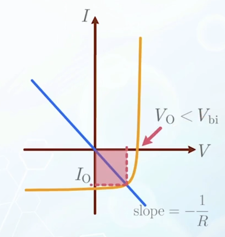
- Shaded area: power
- Maximum voltage from a solar cell is limited by
For silicon based solar cell, usually
Why?
- Fermi level on both side has to be within the bandgap
- Fermi level must align at equilibrium
- It is only possible when
For higher voltage output, multiple cells are connected in series
The current, voltage, and power output provided by a solar cell can vary significantly with the illumination intensity and the load resistance, thus a voltage regulator is usually required to stablize the output voltage
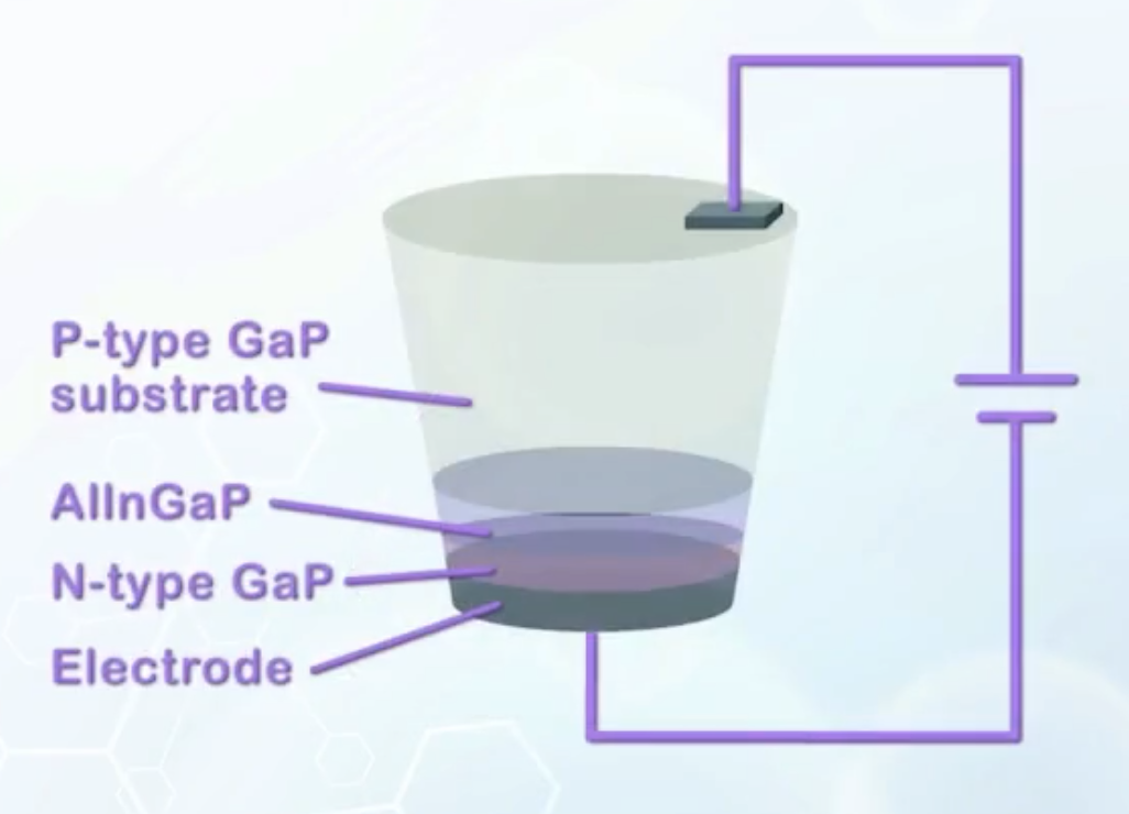
Solar Cell Materials
- Solar cells fabricated using single crystal silicon is still quite expensive
- As single crystal silicon is produced from molten silicon at very high temperature, which is energy intensive and polluting
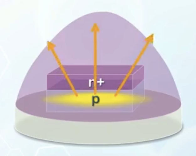
- Light can only penetrate to a small depth from the top, on a PN junction on a wafer surface
- A large portion of substrate material below the penetration depth is only used as mechanical support
- In second generation solar cells, thin film technology is used to form a thin solar cell on a low-cost substrate, usually glass
- Silicon on the supporting substrate is formed by depositing the material using silicon atom carrying gas, such as Silane (
- The deposited film will have either polycrystalline or amorphous structure, due to the mismatch of atomic spacing between the supporting substrate and the thin-film material
- Depositing silicon at low temperature usually leads to amorphous structure, and the grain size increases with temperature
- At sufficiently high temperature, polycrystalline structure can be formed on the supporting substrate
- Grain boundaries exist regardless of polycrystalline or amorphous structure, which cause scattering when carriers move from one grain to another, leading to worse performance than single crystal silicon solar cells
- The thin-film material will also have defects and stability issues
- But the cost is much lower and can cover a much larger area
- Silicon on the supporting substrate is formed by depositing the material using silicon atom carrying gas, such as Silane (
- Third generation solar cells
- Using organic materials
- Low temperature production
- Short turnaround time
- Easy disposal
- Low efficiency
- Low reliability inherent to organic materials
Solar Cell Design
Although solar cells are basically a simple PN junction, some design optimizations are needed to achieve high energy conversion efficiency.
- When light shines on the solar cell, part of the light is absorbed, while part is reflected
- To increase absorption and reduce reflection, an anti-reflection coating is usually applied to the surface
- This is why solar cells look dull from the light absorbing surface
- To increase absorption and reduce reflection, an anti-reflection coating is usually applied to the surface
- To allow maximum amount of light to enter the depletion region, the top layer of PN junction has to be thin, so that the depletion region is closer to the top of the wafer
- The depletion region has to extend deep enough to absorb all the light entering the diode
- This can be achieved by using lightly doping on one side of the junction
- But it also decreases
- To achieve both high
- In this structure, the intrinsic layer will be totally depleted, and the thickness of the intrinsic layer can be used to adjust the depletion width
- On the other hand,
- Contacts have to be added to the top and bottom layers without blocking the light
- So they are usually arranged into strips to minimize the distance from any location on the top layer of the surface of the junction to the metal line
- Another approach is to use transparent electrodes to cover the entire surface
Light Emitting Diodes (LEDs)
- Light is absorbed during electron-hole generation
- The reverse combination process can emit light energy
- A semiconductor can be used as a light source when substantial recombination occurs
- For example, light is emitted in a long PN junction under forward bias because of recombination
- We usually cannot see the emitted light
- Recombination takes place deep inside the silicon crystal
- The energy of emitted photons is, in general, governed by
- Silicon has a bandgap of
- We need materials with larger bandgap to emit visible light
- Organic materials can also be used to form OLEDs
- Silicon has a bandgap of
- Due to the use of large bandgap materials, LEDs usually have a larger built-in potential, thus resulting in a larger turn on voltage
- Typically,
- Typically,
- Designing LED structure to achieve high efficiency
- We want to have all electrons and holes recombine before reaching the end of the diode -> a very long diode
- However, a long diode will push the region of light generation deep inside the solid, making it difficult for light to escape to the surface
- To force more recombination over a shorter neutral region, a heterogeneous structure using materials of different bandgaps is often used

- Electrons and holes are injected and trapped by the higher bandgap material, leading to more recombination in a shorter distance
- All currents are recombination current to ensure efficient conversion from electrical energy to optical emission
- The shape of LEDs also need to be carefully designed
- In most LED applications, light emits only in a particular direction
- Light generated in the LED radiates in all directions
- The bottom surface should be reflective to increase the light intensity in a particular direction of interest
- At the same time, reflection from the top surface should be avoided
- When light reaches the top surface, total reflection may occur if the incident angle is larger than the critical angle, which will reduce the intensity of emitted light
- To avoid total internal reflection
- The semiconductor material may be structured into a dome shape, so that most radiating light will be emitted in a direction perpendicular to the top surface
- Or use some capping material with a similar reflective index to that of the light emitting material, to shape the upper surface
- In case of LED with small light-emitting area, it can be structured like a trapezoid, with slope sides to confine the direction of emitted light
- In most LED applications, light emits only in a particular direction