About the challenges and solutions with short channel MOSFET design, including threshold voltage scaling, source / drain charge sharing, drain induced barrier lowering and punchthrough.
Short Channel MOSFET Design
Besides overcoming fabrication challenges, proper device design is needed to achieve desired performance of small MOSFETs.
The main purpose of a transistor is to serve as an switch, and a good switch should have a high current drive when turned on, and zero when turned off.
When channel length is short, giving high current when turned on is not a problem, the problem is how to turn it off completely.
Consider a long MOSFET with the electric potential of the channel controlled by the gate. When the gate is grounded, energy band in the channel is pulled up, with no electrons flowing in the channel. When drain voltage is applied, it pulls down the band through the drain terminal. There is a competition between the gate terminal holding the band high and drain voltage pulling the band down. In a long channel MOSFET, the gate controls most part of the channel, and the effect of the drain voltage on the channel is very small, so the gate can effectively turn off the MOSFET, holding the energy band high.
However, in a short channel MOSFET, the control of gate voltage over the channel is reduced, due to the its smaller area over the channel. Relatively, the effect of drain voltage on the channel energy band increases, causing the source to body energy barrier to be lowered, and introducing an additional leakage current that cannot be stopped by the gate.
When channel is short enough, the gate loses control of the channel. The MOSFET cannot be turned off, and electron will flow once a drain voltage is applied.
Along the depth of the channel, the gate control is still relatively strong near the gate region. At the bottom od the depletion region under the gate, the body terminal also helps to hold the energy band high when grounded. Therefore, the point that is under the strongest influence of the drain voltage is somewhere between the gate oxide to silicon interface, and the body terminal. The leakage current will be the highest though this particular point.

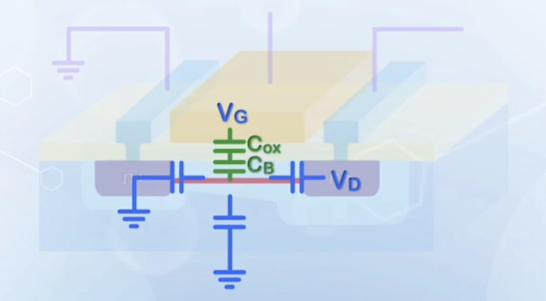
In terms of electrostatic control, when the MOSFET is turned off, the region below the gate is depleted, and is considered insulator. The gate, source, drain and body terminals can only control the potential of the region through capacitive coupling. The potential at any point in the depletion region is the weighted sum of the four terminal voltages, and the relative influence of the terminals are determined by the associated capacitances.
At the channel near the gate, the gate capacitance is
To increase the gate control over the channel
- Increase
- By reducing oxide thickness
- Reduce the depletion region width
- So that the weakest point is closer to the gate
- Effectively, increases
- Using heavy substrate doping
- Reduce the drain capacitance
- By reducing drain junction depth
- Effective side wall area of the drain capacitance is reduced
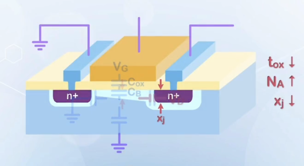
- By reducing drain junction depth
Threshold Voltage Scaling
The choice of
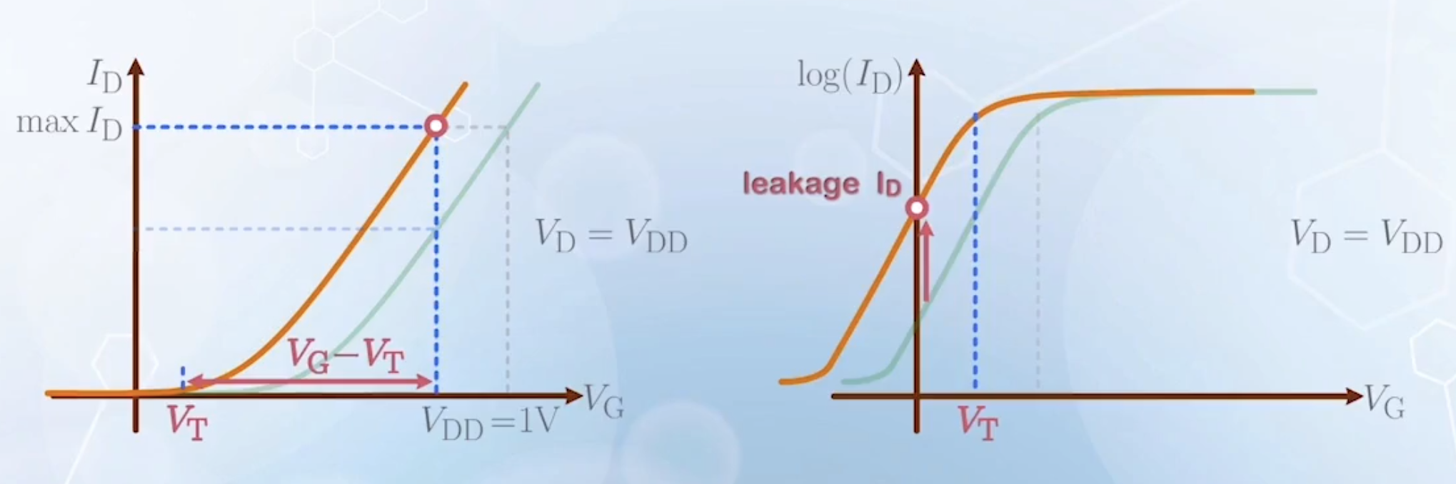
The maximum current drive of a MOSFET is determined by
However, reducing
An Example
Given:
The saturation current:
The leakage current:
To reduce
We can use extremely thin gate oxide to increase
Ideally,
In the past, when calculating transistor power, we only calculate the dynamic power that charges up the loading capacitors. With the reduction of
Source / Drain Charge Sharing
When the channel length is short enough, we say the MOSFET is experiencing short channel effects. The description of the MOSFET becoming a poor switch is qualitative, a more quantitative way is needed to compare the performance of MOSFETs with short channel length behaves differently from long channel MOSFETs.
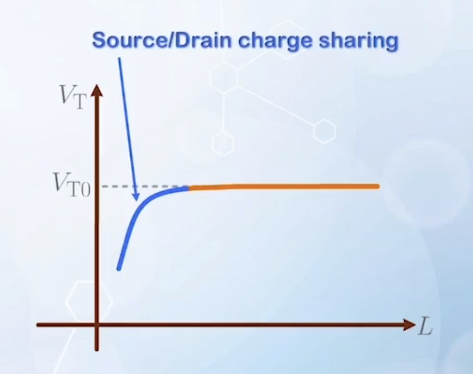
The short channel effect is the dependence of
In classic theory,
Without source and drain, the threshold voltage is given by
The last term is normalized with respect to area. Should be
When source and drain are present, the source and drain depletion region have already depleted some part of the original
Assume
The amount of charge depleted by the source and drain is expressed as
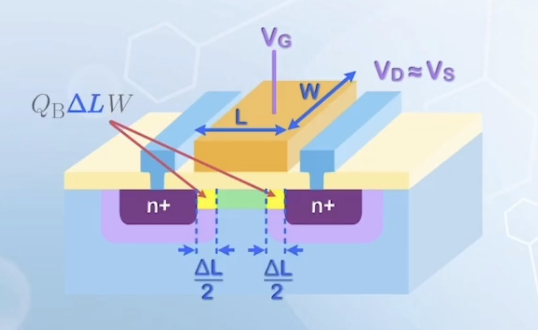
The new threshold voltage is
To put it simply, the source and drain helps the gate by providing some extra charge to the channel, such that a smaller gate voltage is needed to reach the same threshold condition.
In the expression,
Most circuits rely on a stable
To reduce source / drain charge sharing:
- Increase
- The effect of source / drain contributed charge on
- The effect of source / drain contributed charge on
- Decrease
- Reduces the proportion of source and drain depleted charge relative to the gate depleted charge
- Make the source and junction shallower
- Reduces
- Similar to increasing substrate doping to reduce the charge contributed by source and drain
- Reduces
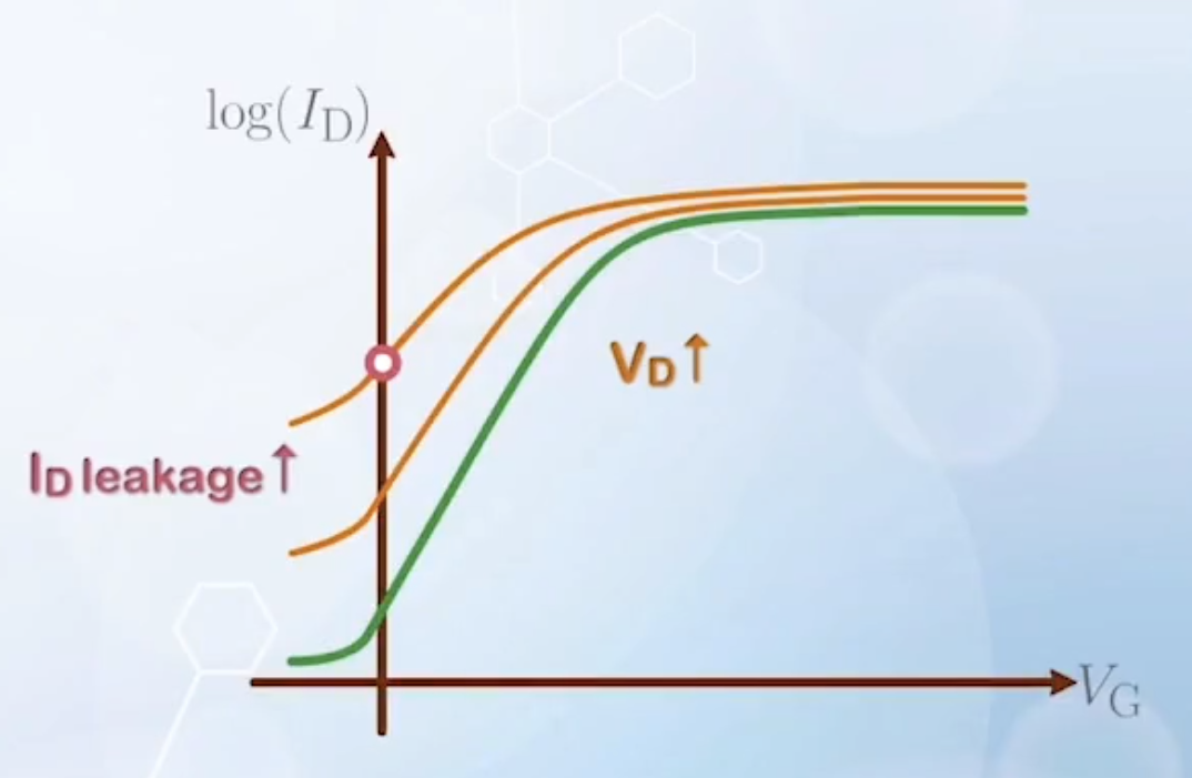
Drain Induced Barrier Lowering (DIBL)
The threshold voltage
To turn on a MOSFET, a gate voltage is needed to reduce the source to channel barrier to cause conduction. In a long channel MOSFET, the drain voltage has limited penetration through the channel, and will not affect the source to channel barrier. When the channel length is short enough, the drain voltage can lower the source barrier. In this case, the gate voltage needed to reach threshold condition is lowered. The higher the drain voltage, the more reduction in the threshold voltage is observed.
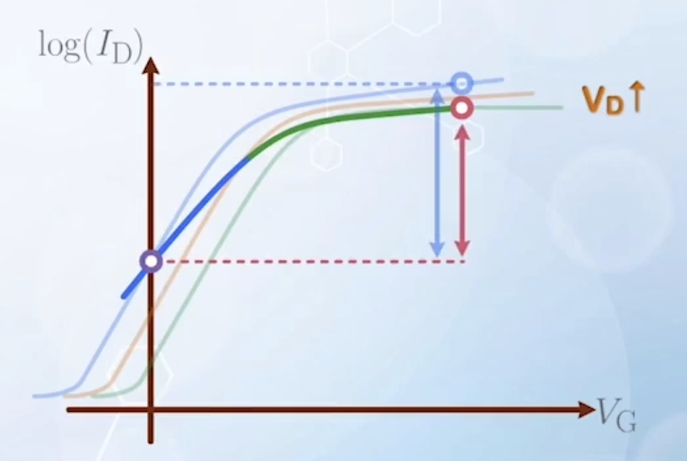
The subthreshold curve of a short channel MOSFET at different
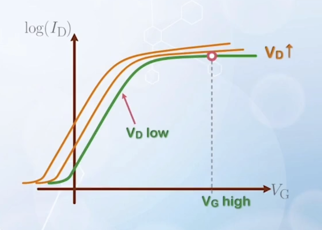
With increasing
The DIBL effect can also dynamically effect the on-off current ratio.
Consider a common CMOS inverter:
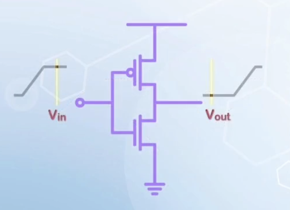
- When input is high, NMOSFET is on, and PMOSFET is off
- Output is pulled to ground
- Drain voltage of NMOSFET is close to ground
- NMOSFET follows the curve with high
- When input is low, NMOSFET is off, and PMOSFET is on
- Output is pulled to
- Drain voltage of NMOSFET is high
- NMOSFET follows the curve with high
- Off state leakage current takes the higher value
- Output is pulled to
- Overall, the NMOSFET follows the low current curve when high current is needed, and the high current curve when low current is needed
- Resulting a much smaller on-off current ratio than that predicted under static condition
- DIBL causes significant degradation in switching performance
To reduce DIBL, it is equivalent to increase the control of gate over the channel
- Reduce oxide thickness to increase
- Increase substrate doping to reduce depletion region width, increasing
- Reduce drain junction depth to reduce drain capacitance
Punchthrough
In DIBL, the drain voltage does not fully lower the source to channel barrier, and the gate terminal still controls the energy band of the region under the gate.
When the channel length is further reduced, the drain voltage may overtake the gate voltage in controlling the energy band under the gate. This is called punchthrough.
The control of gate over the channel decreases along the depth of the depletion region, as the capacitance associated with the gate terminal decreases. When channel length is short enough, some region below the surface may be fully controlled by the drain voltage instead of the gate voltage. The gate has little effect on the energy band at that location, and the conduction is fully controlled by the drain voltage.
With punchthrough, the leakage current increases with increasing drain voltage. Subthreshold swing also increases, as punchthrough weakens the gate control over the drain current. The curve may become flat at high
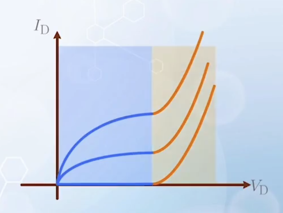
When
To reduce punchthrough, again the gate control over the energy band should be enhanced, while the drain control should be weakened. In addition, the width of drain depletion region should be reduced with heavier substrate doping.
Conclusion
Short channel MOSFETs may become poor switches due to difficulties in turning off. The threshold voltage and the subthreshold swing play an important role in determining the on and off state current of MOSFETs.
In short channel MOSFET design, we want to enhance the gate control over the channel, while reducing the drain control. This can be achieved by
- Thin gate oxide thickness
- Heavy substrate doping
- Shallow source / drain junctions