About charge and capacitance calculation in an MOS capacitor under accumulation, depletion, and inversion modes, and the dynamic capacitance behavior in inversion mode.
Accumulation and Depletion Charge
- Under accumulation mode, the charge is composed of accumulated holes, and is given by:
- Once the gate oxide thickness is given,
- For metal oxide semiconductor
- For N+ polysilicon oxide semiconductor, assume the Fermi level of N+ silicon is very close to the conduction band edge
- For metal oxide semiconductor
- Once the gate oxide thickness is given,
- Under depletion mode, the charge is composed of ionized dopant atoms, and is given by:
- To calculate
- Integrating the Poisson equation in the depletion region gives:
- Once
- The calculation of
- To calculate
- Under inversion mode, the charge is composed of both mobile electrons at the interface, and the ionized dopant atoms in the depletion region:
Calculate Surface Band Bending
To solve the depletion charge, we need to find out what
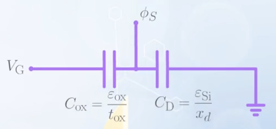
- When an MOS capacitor is operating under depletion mode, the depletion region in the silicon substrate can be considered as another insulator
- The MOS capacitor can be considered as two capacitors connected in series
- One is the oxide capacitor, with normalized capacitance
- The other one is the silicon depletion capacitor, with normalized capacitance
- When
- In the language of engineers,
- With some magical algebraic manipulation, we can obtain an expression of
- By plotting the above expression, and swapping the horizontal and vertical axes, we can obtain a graph of
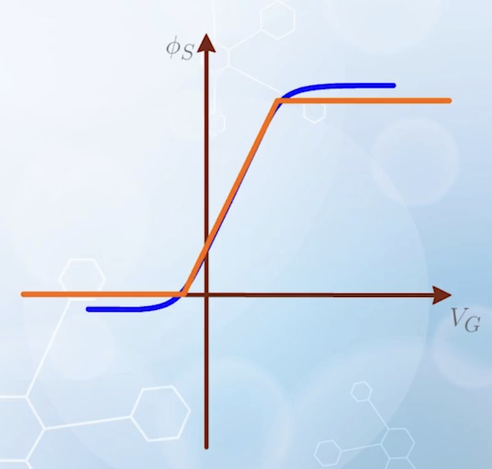
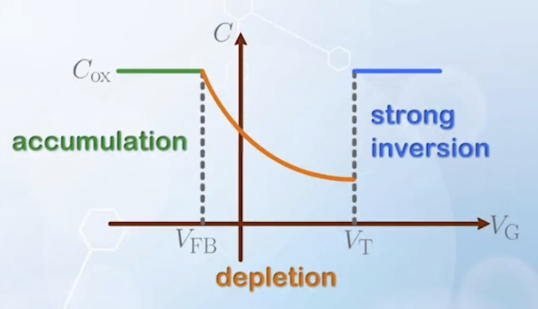
- From left to right
- The first line segment corresponds to the accumulation mode, where
- The second line segment corresponds to the depletion mode
- The third line segment corresponds to the inversion mode
- The first line segment corresponds to the accumulation mode, where
- The two turning points
- In depletion mode,
- The slope can also be derived from the series capacitor model:
- By approximating the slope to be a constant, we sort of assume
- Ideally,
- Happens when
- It is a very important value for MOSFETs
- Happens when
- One is the oxide capacitor, with normalized capacitance
- Now back to
- Finally the depletion charge can be calculated as:
Threshold Voltage and Inversion Charge
In the depletion mode, charge is given by:
We have to obtain
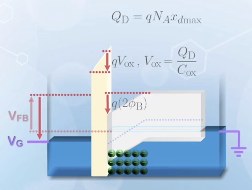
- We give
- We apply additional gate voltage to reach
- The additional gate voltage is dropped across the oxide layer and the silicon depletion region
- The voltage dropped across the oxide layer is
- The voltage dropped across the silicon depletion region is
- The voltage dropped across the oxide layer is
- We now obtain the threshold voltage as
Now we can calculate the total charge in strong inversion mode as a function of
With the expression of
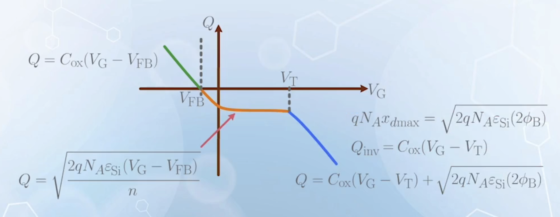
Or, to avoid the polarity, we can plot the absolute value of charge versus gate voltage.
On the gate side, the same amount of charge with opposite polarity is induced, following the dependence of charges in the silicon substrate. The distribution of the charge is assumed to be a sheet charge at the metal-oxide interface.
Equilibrium Capacitance of a MOS Capacitor
The charge in the MOS capacitor generally has very non-linear behavior, thus we need to use the differential form to calculate the capacitance:
To find out the capacitance, the task is to find out where the fluctuating charge
Once done, we can graphically determine the capacitance by treating the location of
- In accumulation mode
- Graphically, the small signal charge
- Graphically, the small signal charge
- In depletion mode
- Graphically, the small signal charge
- As the depletion width
- The shape is similar to the capacitance of a reverse-biased PN junction, but inversed horizontally because the voltage is applied on the gate side (N+ side)
- They both come from the fact that the depletion width increases with higher biasing voltage
- As the depletion width
- Graphically, the small signal charge
- In inversion mode
- Graphically, the small signal charge
- Graphically, the small signal charge
The capacitance-voltage characteristics of an MOS capacitor can be plotted as:
This is a simplified model. The actual
Dynamic Capacitance in the Inversion Region
The
- To measure the MOS capacitance, a DC ramp-up voltage is applied, to define the biasing conditions on the voltage axis of the graph
- A small AC signal is superimposed to the system to measure the capacitance
- The DC ramp-up voltage can be fast or slow, the same for the AC measurement signal frequency, so there are four possible measurement setups
- When both the DC and AC signals are slow, the measured capacitance is the equilibrium capacitance described above
- When the DC signal is slow, but the AC signal is fast
- The capacitance remains the same after reaching the threshold voltage
- When both the DC and AC signals are fast
- The capacitance continues to decrease after reaching the threshold voltage
- The condition with fast DC signal but slow AC signal does not make sense, because if the DC signal ramps up before the AC signal can finish a cycle, the AC signal is no longer considered AC
- The resistance is very high in the conduction band, electrons cannot be supplied from the conduction band. The electrons are supplied by thermal generation
- When the holes are depleted by
- More electrons are generated, and holes are removed through the ground terminal connected to the substrate
- The current path is though thermal generations and majority carrier motions in the valence band
- When the holes are depleted by
- The thermal generation process is relatively slow, in range of milliseconds
- If measurement is performed using frequencies higher than
- If electrons cannot be generated fast enough, the depletion region will continue to expand beyond
- When ramp-up stops, the system will stabilize, electrons will be generated, and depletion width will return to
- When the ramp-up is slow, the band diagram is allowed to stabilize, and depletion width is kept at
- When slow AC signal is applied, electrons can be generated or removed through thermal generation and recombination, the equilibrium capacitance
- When fast AC signal is applied, there is no time for generation and recombination, thus more holes will be depleted or recovered at a distance of
- When slow AC signal is applied, electrons can be generated or removed through thermal generation and recombination, the equilibrium capacitance
- When the ramp-up is fast, the band diagram cannot stabilize, and depletion width continues to expand beyond
- The measured capacitance will be smaller thant the equilibrium capacitance in the threshold condition
- The depletion width will increase with larger
- Also called the deep depletion mode
- What is high frequency?
- It depends on the thermal generation rate
- For a good silicon crystal, it is in the
- Compared with modern electronics operating in
- Additionally, we seldom do measurements at such low frequencies, as the result may be easily disrupted by physical noises such as vibration
- Most measurements are done at a frequency of
- The low frequency