2024 年 1 月寒风吹彻
半导体器件原理 2.5 Classical MOSFET Turn-on Current

半导体器件原理 2.5 Classical MOSFET Turn-on Current

2025 年 11 月 24 日

About how to calculate the current of a MOSFET when it is turned on, based on the classical pinchoff model, the channel length modulation effect, and some discussions about the inconsistencies and limitations of the model.


Charge and Velocity of Channel Carriers

MOSFET is basically a switch controlled by gate. When VG<VT, electrons from the source cannot enter the channel, and no current flows. When VG>VT, electrons from the source can enter the channel, and a conduction path is formed. A current will flow if a positive VG is applied (NMOSFET).

NMOSFET structure

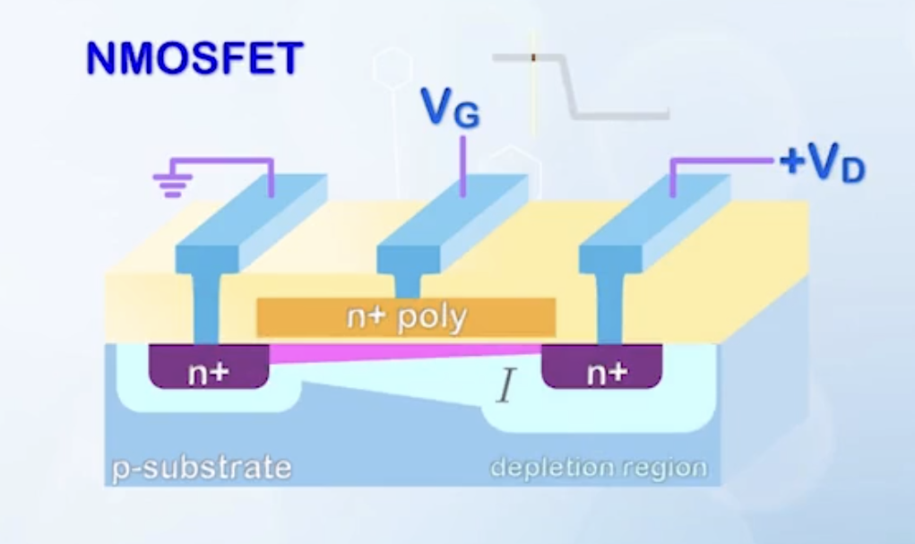
Assume source and substrate are grounded

  • As a switch, ID is mostly assumed to be 0 when VG<VT
  • When VG>VT, inversion electrons form in the channel, and electrons will be attracted from the source to drain by the positive VD
    • The electric field is the main driving force, and the current is mainly drift current
    • The current depends on the number of charge available, and the velocity of these charges
    • The current at any location y isI(y)=Q(y)v(y)where Q(y) is the amount of charge at location y
    • Defining y as the coordinate from the source to drain
    • There is no accumulation or removal of charges, the current flows remains constant along the channel
      • The region with more charges will have lower velocity, and vice versa
    • Starting from a small VD close to 0
      • For a MOSFET with channel length L and width W, total charge under the gate isCoxWL(VGVT)
      • The charge per unit length is the above divided by LQ(y)=CoxW(VGVT)
    • When VD increases, the voltage across the gate capacitor near the drain will be reduced to VGVD, so the charge per unit length near the drain becomesQ(y)=CoxW(VGVTVD)which means, the charge near the drain is less than that near the source
      • The voltage in the channel somewhere between source and drain is V(y), so the charge per unit length at location y isQ(y)=CoxW(VGVTV(y))VT should be a function of y, as increasing V(y) is similar to decreasing VD, but the effect is ignored for now
    • The velocity of electrons are usually assumed to be proportional to the electric fieldv(y)=μE(y)where μ is the mobility of carriers. For electrons in siliconμe(b)=1400cm2V1s1It is the mobility when electrons are moving inside the bulk silicon
      • When electrons are moving near the silicon-oxide interface, the mobility is lower due to more scatteringμe(s)=600cm2V1s1
      • For holes in siliconμh(b)=450cm2V1s1μh(s)=250cm2V1s1
    • The current is given byID=CoxW(VGVTV(y))μE(y)

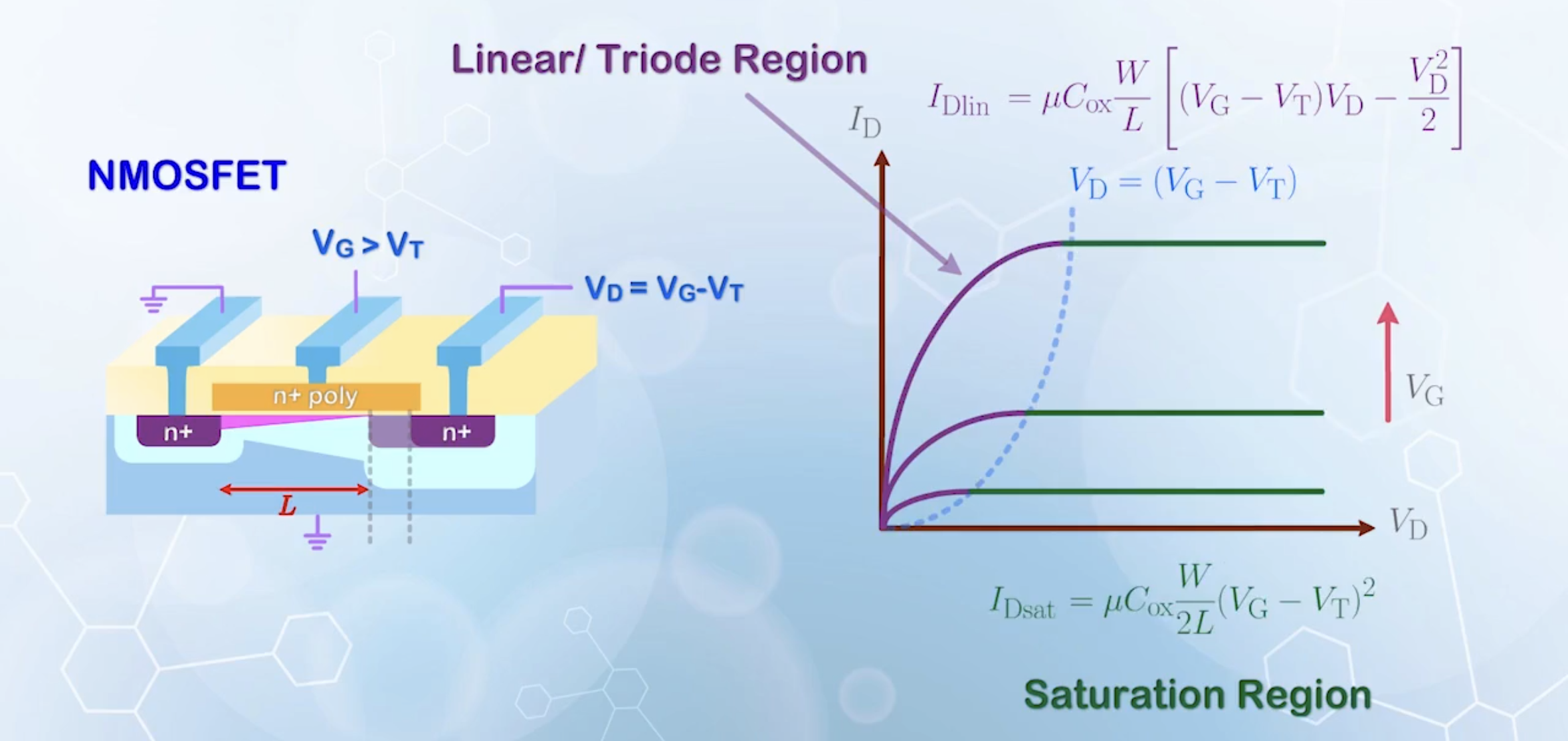
Linear Region Current Equation

  • The electric field is the negative gradient of voltage

    E(y)=dV(y)dy
  • Now the current equation becomes

    IDdy=CoxWμ(VGVTV(y))dV(y)

    There should be a negative sign in the equation, but let’s focus on the magnitude for now

  • Integrating both sides from source to drain

    sourcedrainIDdy=sourcedrainCoxWμ(VGVTV)dV0LIDdy=0VDCoxWμ(VGVTV)dVIDL=CoxWμ[(VGVT)VDVD22]ID=μCoxWL[(VGVT)VDVD22]
  • A simpler approach is

    • The current is also given byID=Qavgvavg
    • The average charge per unit length is just the average of the charge at source and drainQavg=CoxW(VGVTVD2)
    • As of the average velocityvavg=μEavg
    • If we assume the electric field is uniform along the channelEavg=VDL
    • In reality, the electric field near the source is lower, and that near the drain is higher, as electrons move faster near the drain
    • However, integrating E over the channel length must give VD still, so the average electric field is still VD/L
    • Therefore,ID=CoxW(VGVTVD2)μVDLwhich is the same as the previous result

Saturation Region Current Equation

As VD increases, ID will increase until VD=VGVT. If we still follow the previous current equation, when VD exceeds VGVT, the current will start to decrease, and eventually become 0. But from measurements, the current of a MOSFET eventually saturates and becomes a constant with a high enough VD.

  • For the inversion charge distribution

    CoxW(VGVTV(y))

    to be valid, VGVTV(y) must be positive. Otherwise, the channel will be depleted, and there will be no charge for conduction

    • This will happen at the drain when VD becomes larger than VGVT

    • A pinchoff region, where the channel is depleted, will form near the drain

    • The channel can be separated into two different regions by the V(y)=VGVT point

      • Gradual channel region: the region where V(y)<VGVT, inversion charge exists, and the channel behaves like a conductor
      • Pinchoff region: the region where V(y)>VGVT, inversion charge is depleted, and the channel becomes an insulator
    • All drain voltage beyond VGVT will be dropped across the pinchoff region

    • !!!INCONSISTENCY MENTIONED!!!

      In the pinchoff region, the channel is depleted, and Q(y)=0. Meanwhile, the current is given by ID=Q(y)v(y). How can there be a current if there is no charge?

      This inconsistency will be resolved later, and for now, we just forget about the pinchoff region, and assume the drain is moved to the VGVT point, with VD picking up the value of VGVT.

    • Assuming the pinchoff region is very small compared to the channel length, and the length of the gradual channel region can be approximated as L

    • Then, the current in the pinchoff condition is calculated with the same equation as before, but with VD replaced by VGVT

      IDsat=μCoxWL[(VGVT)(VGVT)(VGVT)22]=12μCoxWL(VGVT)2

      Any VD beyond VGVT will be dropped across the pinchoff region, and will not affect the current

  • Therefore, the final current equation is

    IDlin=μCoxWL[(VGVT)VDVD22]VD<VGVTIDsat=12μCoxWL(VGVT)2VDVGVT
    • The first region is called the linear region or triode region, and the second region is called the (current) saturation region
    • The separation between the two regions isVDsat=VGVT

    NMOSFET I-V characteristics

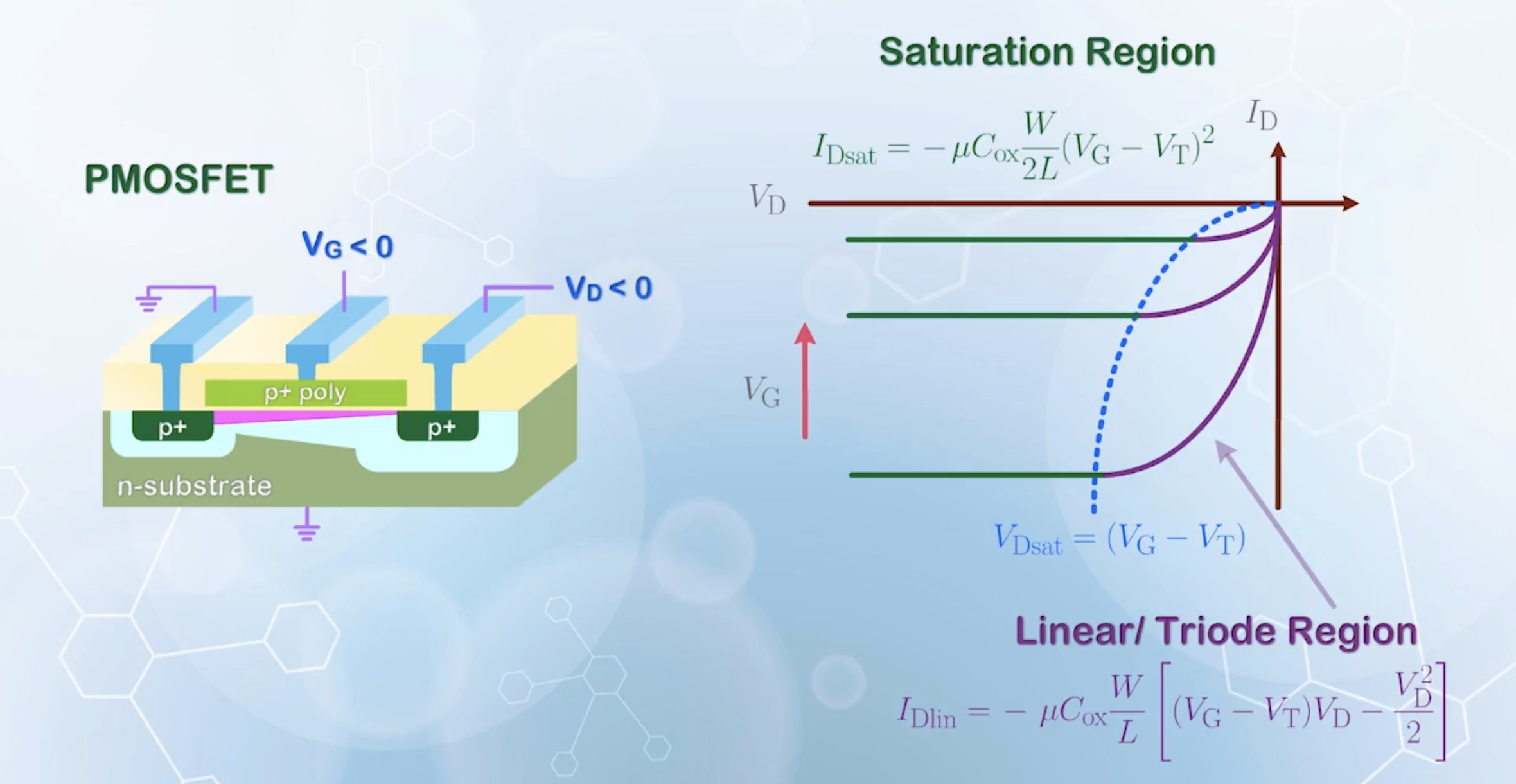
  • Same applies to PMOSFET, with voltages and currents become negative relative to the source

    • Negative sign is added to the current, as the current in PMOSFET flows out of the drain

    PMOSFET I-V characteristics

Channel Length Modulation

Previously, we assumed the drain voltage beyond VDsat does not affect ID. However, in reality, increasing VD beyond VDsat will extend the pinchoff region further into the channel, and the length of the gradual channel region will be reduced. As a result, ID will increase. This is the channel length modulation effect, describing how VD affects ID by changing the effective channel length.

  • In saturation region, the current is given byIDsat=12μCoxWLch(VGVT)2where Lch is the length of the region where the channel voltage increases from 0 to VDsat
  • Replacing Lch with LΔL, and perform some mathematical magic, we haveIDsat=12μCoxWLΔL(VGVT)2=12μCoxWL11ΔLL(VGVT)2=IDsat011ΔLL=IDsat0(1+ΔLL+(ΔLL)2+)IDsat0(1+ΔLL)ΔL is assumed to be very small
  • To calculate ΔL, we use Poisson’s equation
    • In the pinchoff region, there are only the depleted charge from the dopant ions
    • Therefore, the charge density isρ=qNA
    • Integrate twice to get the voltage difference across the pinchoff regionV=qNA2εSi(ΔL)2
    • The voltage across the pinchoff region is VDVDsat
    • Thus,ΔL=2εSiqNA(VDVDsat)
    • Putting it backIDsat=IDsat0(1+1L2εSiqNA(VDVDsat))
    • !!!INCONSISTENCY BACK AGAIN!!!

      For the same reason mentioned before, ΔL given here is physically incorrect, as assuming the pinchoff region only contains depleted charge is physically incorrect.

  • IDsat has a square root dependence on VD beyond VDsat
  • As the range of VD is limited, we can linearize the equationIDsatIDsat0(1+λVD)where λ is the channel length modulation parameter
  • The slope in the IDVD curve is then given by IDsatλ, and the output resistance isro=1λIDsat0which is similar to the output resistance of a BJT, which is given byro=VAICwith VA replaced by 1/λ and IC replaced by IDsat0
    • Therefore, 1/λ is sometimes called the VA of a MOSFET, and the unified output resistance equation isro=VA+VDIDsatVAIDsatassuming VAVD

Inconsistencies in the Pinchoff Model

We have derived different equations for the MOSFET current in linear and saturation regions based on the pinchoff model.

  • For VD<VGVTIDlin=μCoxWL[(VGVT)VDVD22]
  • For VD>VGVTIDsat=12μCoxWL(VGVT)2(1+λVD)
  • There are some inconsistencies
    • Mathematical inconsistencies: using the two equations, the current at VD=VGVT is not continuous
      • Actually, the equation given for the saturation region is only used to illustrate the effect of VD on ID, and is never used to calculate IDsat besides finding the slope after differentiation
      • The simplest way to correct for the discontinuity is just substitute VD with VDVDsat, but who cares?
      • We just assume the channel length modulation effect is very small, and use IDsat0 to approximate IDsat
    • Physical inconsistencies: according to the pinchoff model, Q(y)=0 for y in the pinchoff region. To obtain a finite current, v(y) must be infinite. However, based on the knowledge of relativity theory, the speed of light is the limit of all measurable speed, so the velocity of electrons cannot be infinite
  • However, it is still a good approximation to reality in some special cases
  • These are the limitations of the pinchoff model, more accurate models will be discussed later

文件历史

refactor: general refactoring c2feee5
2025 年 11 月 29 日 08:49djdjz7
content: principle of semi devices 2.5 6e7dad1
2025 年 11 月 24 日 08:56djdjz7
© 2023 - 2025
Unless otherwise stated, text contents are licensed under CC BY-NC 4.0, and codes are licensed under MIT.
Images may be subject to separate licenses, see the image captions for details if applicable.