About the subthreshold behaviors of MOSFETs, the turn-on characteristics, comparison between MOSFETs and BJTs, and the effect of body bias and substrate depletion charge on MOSFET I-V characteristics.
MOSFET Subthreshold Region
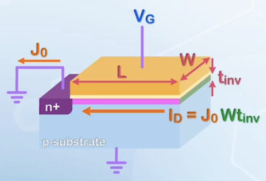
For a properly designed MOSFET, the
We have derive the current equation for MOSFET when
- Consider the potential barrier
- When
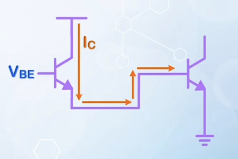
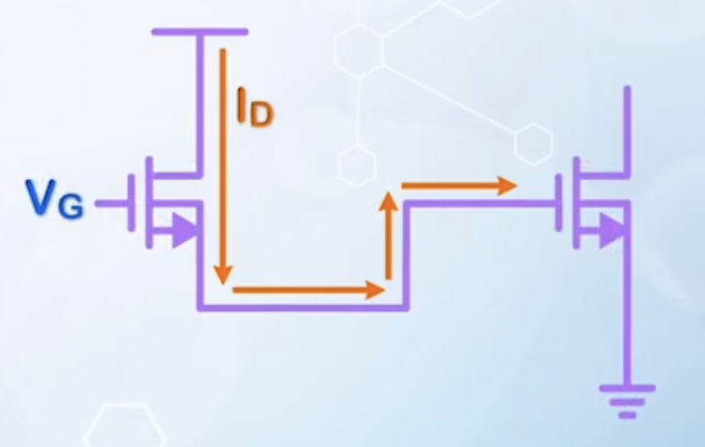
- Before the MOSFET turns on, it is similar to a BJT, with
- In a BJT, the collector current under forward active mode is given by
- Similarly, the subthreshold current of a MOSFET can be expressed as
- When
- From previous section, we know that in depletion region,
- The subthreshold region also operates in depletion region, as we have
Turn-on Characteristics
We have now obtained all the equations for drain current of a MOSFET from subthreshold to strong inversion, we can now study the characteristics of a MOSFET when it is turned on or off with
Plotting the
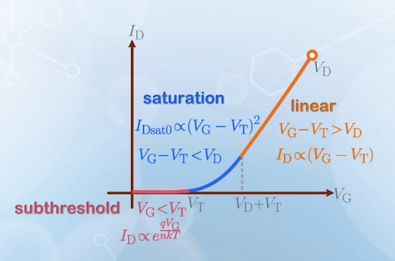
- Before
- Because the current is relatively small in this region, it is difficult to observe its characteristics in a linear scale
- After
- After
- When measured with a larger
- The curve remains more or less the same in subthreshold and saturation region, because
- The linear region extends further, as the transition point
- The curve remains more or less the same in subthreshold and saturation region, because
- There are some similarities between this graph, and the
- The turn-on voltage for silicon junctions is assumed to be
- The turn-on voltage for silicon junctions is assumed to be
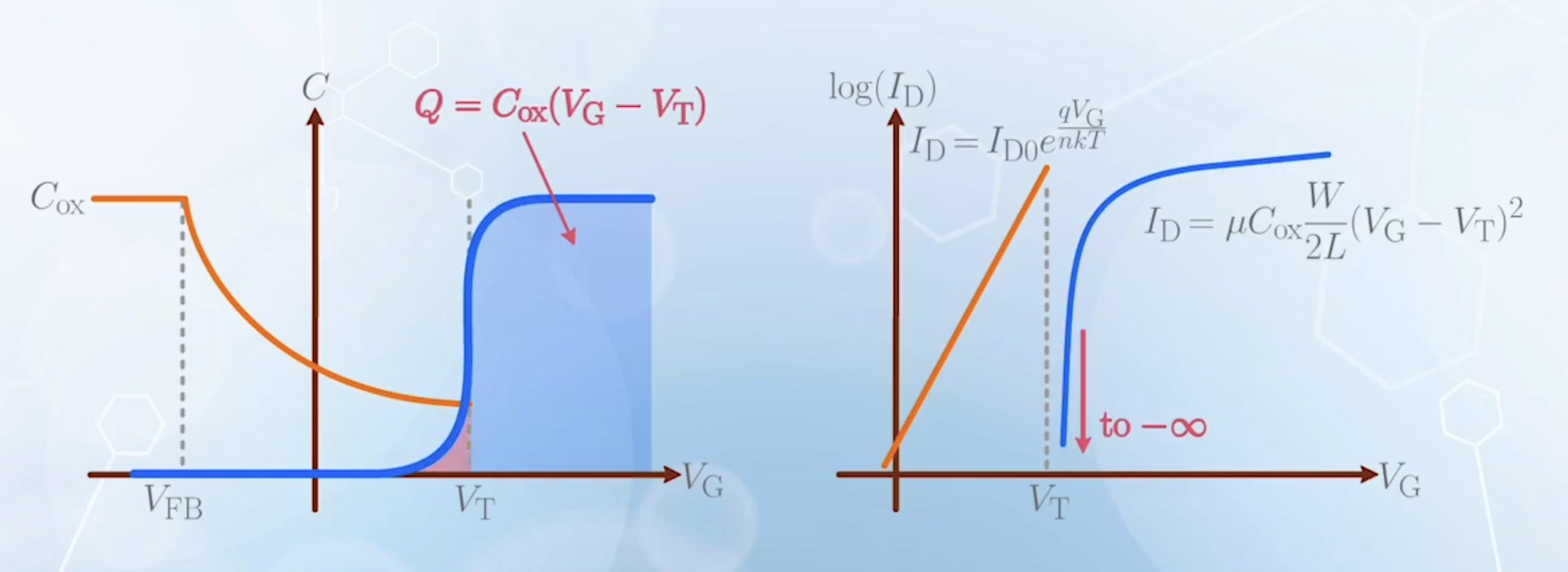
- To observe the subthreshold characteristics more clearly, we can plot the same data in a semi-log scale
- The subthreshold region now becomes a straight line, showing the exponential dependence of
- It is similar to the BJT Gummel Plot, or the
- The part beyond
- In MOSFET, we can use this region, as the gate blocks the current with the insulating oxide
- The part beyond
- The slope of the subthreshold region is
- At room temperature, the subthreshold swing is approximately
- At room temperature, the subthreshold swing is approximately
Subthreshold Swing
The subthreshold swing indicates the ratio between the on state current and off state current of a MOSFET. This is because once
- For example,
- This means for every
- From
- If
- This means for every
- The actual leakage current may be larger than the predicted value due to other effects
- The leakage current from the drain to substrate may define the lowest bound of the leakage current
- This current is independent of
- This current is independent of
- The leakage current from the drain to substrate may define the lowest bound of the leakage current
- As
- This can be done by maximizing
- Reducing
- It is more common to increase
- Reducing
- The best achievable subthreshold swing at room temperature is approximately
Similar to the linear plot,
Current at the Threshold Voltage
Combining the subthreshold current equation and the strong inversion equations, we will observe a discontinuity at
This discontinuity occurs because we used
In reality, the inversion charge appears before threshold, as there are always electrons in the conduction band to prevent the current at
Handling the current at
The main takeaway of this section is that there is a small region around
MOSFET v.s. BJT
BJTs and MOSFETs are usually considered very different devices operating with different principles. However, are actually very similar. They are both comprised of the sam PNP / NPN structure, and MOSFETs in subthreshold region operates very similarly to BJTs.
When considering the performance of a device, we not only consider its output, but also the loading device introduced to operate it. More specifically, the speed of a device is determined by the speed to charge the input capacitance of similar devices to the required voltage through its current.
If input capacitance is
Or the speed can be characterized by
- Consider a BJT driving itself
- Assume a specific current density
- The size of a BJT is mainly determined by the emitter area given by
- The current flows vertically, and is given by
- The input capacitance is mainly determined by the base-emitter junction capacitance
- The capacitance is given by
- The speed:
- Reducing the size of the BJT does not affect its speed, as both current and capacitance scale with area
- Assume a specific current density
- Consider a MOSFET driving itself
- Assume it has the same current density
- The input capacitance is
- However, the current flows horizontally through the channel, with a cross-sectional area of
- The current is given by
- The speed:
- Because
- To increase the speed, we have to either increase the current drive, or decrease the loading capacitance
- This is why we operate MOSFETs at a higher
- This is why we operate MOSFETs at a higher
- Early day MOSFETs operating in subthreshold region have such a low driving current that they are considered not usable for any meaningful applications
- When we scale down the MOSFET,
- In SOTA MOSFETs,
- The increase in speed when scaling down is mainly contributed by the reduction of loading capacitance, instead of the increase in current, making MOSFETs suitable for integrated circuits with closely packed transistors and small parasitic capacitive loading
- When driving external elements with high capacitive load, BJTs with large cross-sectional area is still more desirable
- This is why BJTs are more popular as a discrete element to function as a driver for large external loads
- Assume it has the same current density
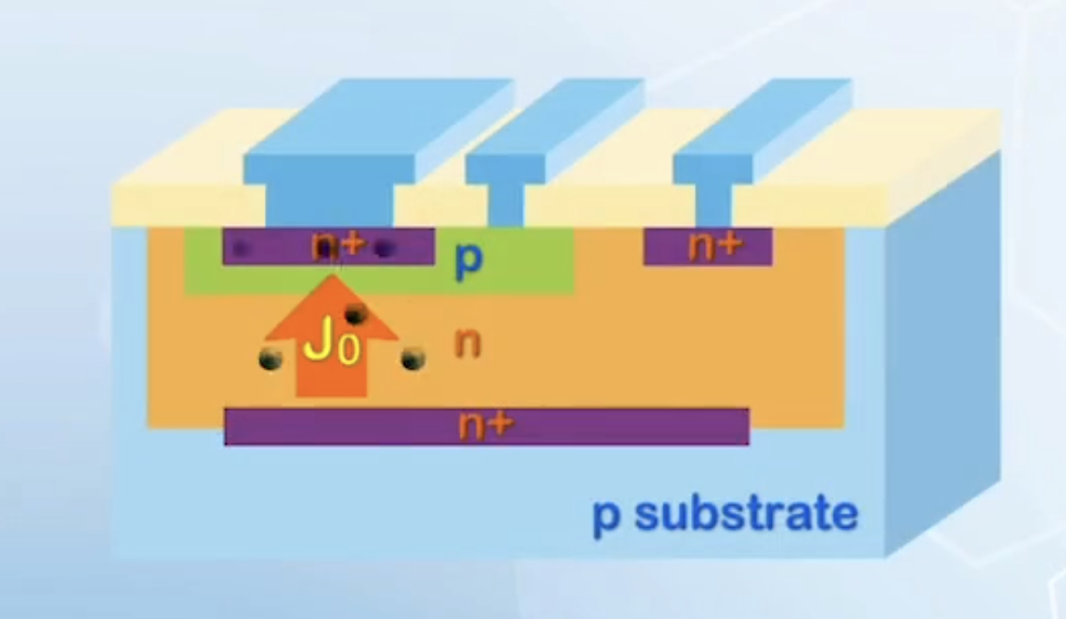
I-V Characteristics with Substrate Bias
Up to now, we have assumed that the source and substrate of a MOSFET are connected together and grounded. However, in some applications, like source follower circuits, source voltage may be higher than the substrate voltage, or effectively a negative substrate bias is applied to the MOSFET.
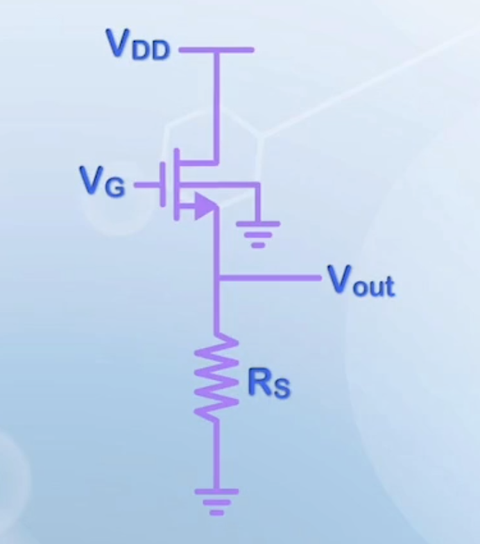
- When source and body voltages are different, we need to pick a reference
- In the source follower circuit, we can pick the source voltage as reference, and
- The
- Or we can pick the source voltage as reference
- Label
- In MOSFETs, we are more interested in the inversion electrons in the channel, and these electrons come from the source, thus this reference is more commonly used
- The
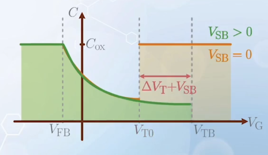
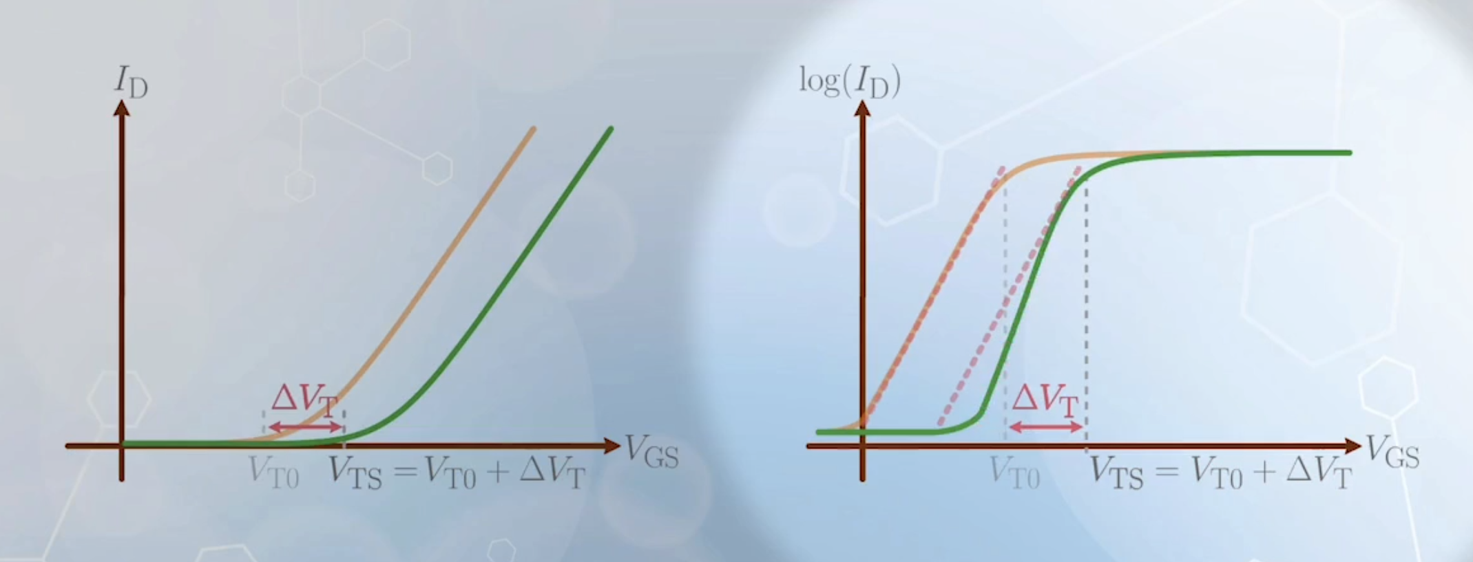
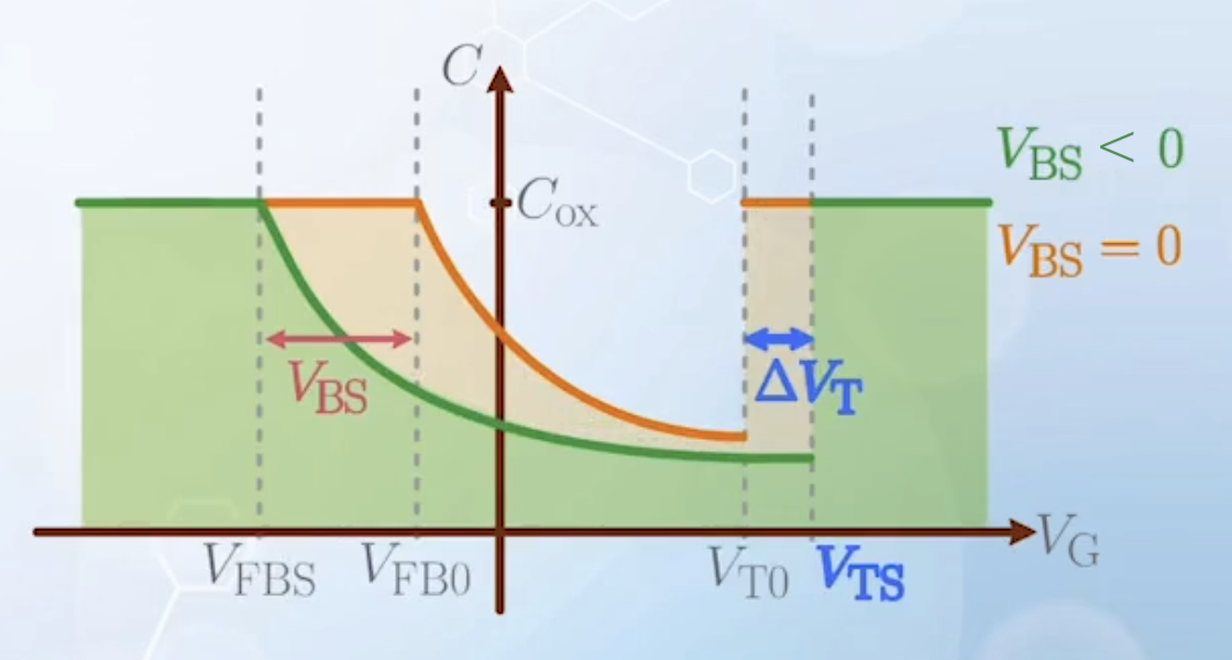 Its effect is mainly the change in
 - The
- As the capacitance with body bias in the depletion mode is smaller compared to no body bias, and the capacitance is a series of
- Label
- In the source follower circuit, we can pick the source voltage as reference, and
Substrate Depletion Charge Effect
When deriving the current equations of MOSFETs, we have assumed
However, this is not true, and
Putting it back to
Again, we assume the range of
and
Following the previous derivation steps, we can get
Usually,
which means the equation assumes
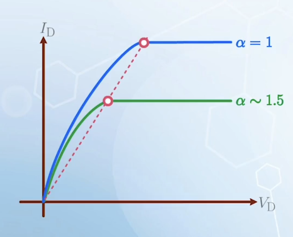
After modifying the linear region, we also need to modify the saturation region, just by finding the peek of the quadratic equation.
In traditional long channel transistors,
No matter the value of
The change in