2024 年 1 月寒风吹彻
半导体器件原理 2.7 Mobility Degradation and Carrier Velocity Saturation

半导体器件原理 2.7 Mobility Degradation and Carrier Velocity Saturation

2025 年 11 月 25 日

About mobility degradation in MOSFETs, and the carrier velocity saturation model.


Effect of Gate Voltage on Carrier Motion

The previous given equations to calculate ID have assumed that the carrier mobility μ is a constant and bias independent. However, for carriers moving near the interface between the bulk silicon and the gate oxide.

Electrons moving in the channel are under the influence of two electric fields: the vertical field from the gate, attracting it to move vertically towards the gate oxide, and lateral field from the drain, attracting it to move laterally towards the drain.

The electron will bounce off the silicon and oxide interface a few times before reaching the drain. If the vertical field is strong, electrons will bounce more times off the surface. The collision between the electron and the interface is inelastic, causing energy loss and reducing the velocity of the electron. Therefore, it will take longer time for electrons to reach the drain.

Thus, the mobility μ is not a constant, and decreases with an increasing vertical field, or increasing VG. This is the mobility degradation due to vertical electric field.

To correct for this effect, μ need to be modified as μ(VG).

The Effective Vertical Electric Field

To quantify the variation of μ caused by VG, we need to calculate the vertical electric field.

Electrons at different distance from the interface will experience different vertical electric field. To simplify the problem, the average electric field is used, assuming it to be the electric field experienced by all electrons.

  • x: the distance from the interface into the bulk silicon, in the vertical direction
  • n(x): the electron concentration at location x
  • Ex(x): the vertical electric field component Ex at location x
  • The average vertical electric field isEeff=n(x)Ex(x)dxn(x)dx=Qinv2εSi+QBεSiwhere Qinv is the inversion charge density, and QB is the depletion charge density, relabeled from QD in the MOSFET capacitance section to avoid confusion with the drain charge
    • An intuitive derivation of this equation:
    • The average electric field can be considered the electric field experienced by an average electron
    • The average electron is the one with half of the electrons in the channel above it, and half below it
    • The electric field starts at a positive charge at the game, and terminates at a negative charge at the substrate
    • Electric field terminating above the average electron will not be experienced by the average electron
    • Therefore, only the electric field terminating below the average electron will be experienced by the average electron
    • Once the charge Q terminating the electric field below the average electron is known, the electric field can be calculated as E=QεSi
    • The charge Q is comprised of two parts:
      • Half of the inversion charge Qinv, since only half of the electrons are below the average electron
      • The entire depletion charge QB, since the inversion layer is very thin compared to the depletion region
    • Thus the equation is obtained
  • We need to further express Eeff as a function of VG
    • The inversion charge density isQinv=Cox(VGVT)
    • The depletion charge can be calculated with the following equationVT=VFB+2ϕB+QBCoxas the threshold voltage VT can be obtained from measurements rather than calculationQB=Cox(VT(VFB+2ϕB))approximating ϕB=0.35Vand VFB=(0.55V+ϕB)VFB+2ϕB=0.2V=VaQB=Cox(VT+Va)Va is dependent of gate material and substrate doping
    • The effective vertical electric field can now be expressed asEeff=Cox(VGVT)2εSi+Cox(VT+Va)εSi=εox(VGVT)2εSitox+εox(VT+Va)εSitoxapprox. εSi=11.9ε03εox=3×3.9ε0Eeff=(VGVT)6tox+(VT+Va)3toxwhere Va=0.2V
    • Once VG, VT and tox is known, the effective vertical electric field can be calculated

Calculating Effective Mobility

We still need to obtain the relation between μeff and Eeff.

There are many theories predicting the effective mobility based on the microscopic effects, but none of them fit the experimental data well.

In practice, engineers rely on experimental calibration to obtain the effective mobility. Experimental data are collected are plotted:

mu_eff versus E_eff

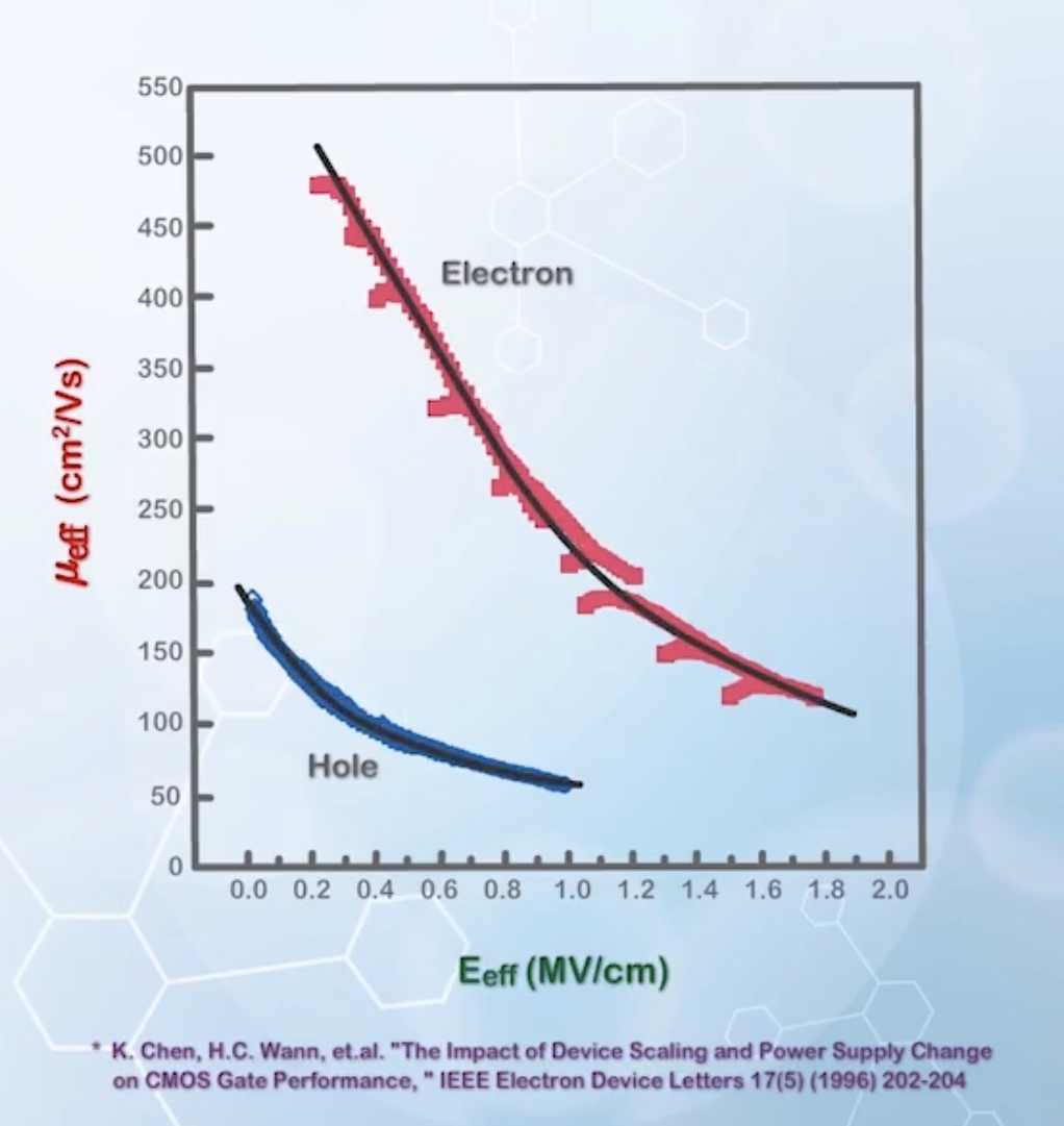
Regardless of the gate oxide thickness and the substrate doping concentrations, they all fall onto a single curve.

As the results are very consistent, an empirical equation is more practical to use, rather than complex theoretical models.

The empirical equation is given as

μeff=μ01+(Eeff/E0)ν

and a widely used set of parameters for this model is

ElectronsHoles
μ0(cm2/(Vs))670160
E0(MV/cm)0.670.7
ν1.61.0

Some other sets of parameters are also used, due to variations in the fabrication process and the physical structure.

This is the universal mobility model, as it can fit different sets of data very well.

The relationship between
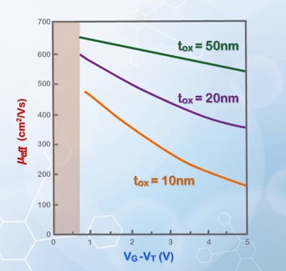
 μeff and VGVT can be expressed as

μeff=μ01+((VGVT)6E0tox+(VT+Va)3E0tox)ν

Now we can plot μeff versus VG for different oxide thicknesses:

mu_eff versus V_G with different oxide thickness

Note that the model may not be accurate for VG close to VT, as we use Cox(VGVT) to approximate the inversion charge, giving 0 at VG=VT, which is not true, as discussed in previous sections. But for most of the part, it is valid.

From the graph, we can see that when tox is large, assuming μ to be a constant won’t introduce significant error. But when tox is small, using a constant μ will introduce an error of more than 50% at high or low VG values. This is because for a given power supply voltage Vdd, the range of VG is fixed, and according to the equation of Eeff

Eeff=(VGVT)6tox+(VT+Va)3tox

thinner oxide thickness will lead to larger Eeff variation for the same VG variation, causing larger μeff variation.

Therefore, the mobility degradation effect may not be important for older MOSFETs with thick oxide, but it is very important for modern MOSFETs with thin oxide.

The IDVG and IDVD characteristics considering mobility degradation is shown below:

I_D versus V_G and I_D versus V_D considering mobility degradation

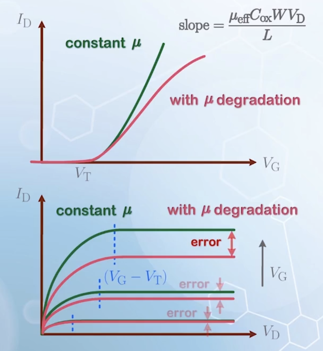
Compared to constant μ, mobile degradation will cause a downward bending in the IDVG curve, as opposed to the linear increase in the constant μ case. And in the IDVD curve, all current will be overestimated if mobility degradation is not considered, with larger error at higher VG.

Carrier Velocity Saturation Model

Up to now, we have linearly related the carrier velocity v to the electric field E

v=μeffE

E is given by VDd, and can be very large when d is small enough, without a theoretical limit. The maximum achievable electric field is determined practically by the strength of the medium, and a discharge will occur if the medium cannot withstand the electric field. However, the speed of carriers is bounded by the speed of light, according to the theory of relativity. Therefore, the linearity between v and E cannot hold forever, and the velocity will saturate with a high enough E. This is carrier velocity saturation.

Carrier velocity saturates with high enough E

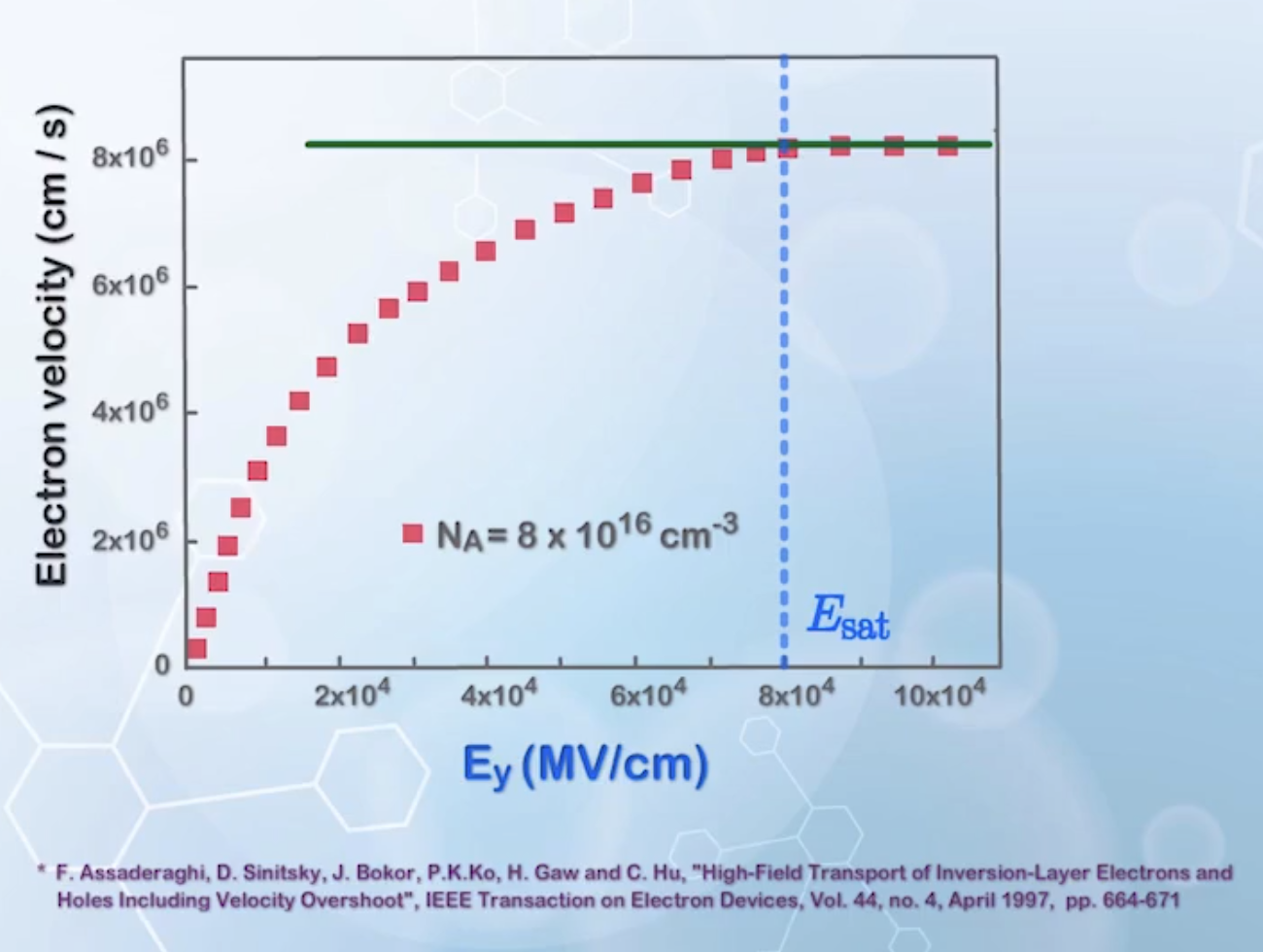
From measurements, carrier velocity saturates at a certain electric field Esat, and the saturated velocity for electrons and holes are approximately

electronsvsat8×106cm/sholesvsat6×106cm/s

To include this effect in drain current calculation, we need to derive a new expression for carrier velocity v=f(Ey) with respect to the lateral electric field Ey.

The easiest way is to use a straight line to connect the two known points: (0,0) and (Esat,vsat), giving

v={μEyEy<EsatvsatEyEsat

To be more accurate, the slope of the curve, or mobility, should decrease when the lateral electric field increases, so a better expression would be

v={μeff1+EyEsatEyEy<EsatvsatEyEsat

The slope will be decreasing with increasing Ey

slope=dvdEy=μeffEsat2(Esat+Ey)2slope|Ey=0=μeffslope|Ey=Esat=μeff4

providing better fitting for the data.

We have the measured vsat, so Esat can be calculated as

vsat=μeff2EsatEsat=2vsatμeff

where μeff is given by

μeff=μ01+(Eeff/E0)ν

To derive the new drain current equation considering velocity saturation

ID=Q(y)v(y)=CoxW(VGVTV(y))μeff1+dV/dyEsatdVdyIDdy=(μeffCoxW(VGVTV(y)IDEsat)dV0LIDdy=VSVD(μeffCoxW(VGVTV(y)IDEsat)dVIDL=μeffCoxW[(VGVT)VD12VD2]IDEsatVDIDlin=μeffCoxWL[(VGVT)VD12VD2]1+VDEsatL

Compared to the classical model, there is just an additional factor of 11+VDEsatL.

As for the saturation region, we define VDsat as the drain voltage that causes the lateral electric field near the drain to reach Esat

IDsat=WCox(VGVTVDsat)vsat

VDsat is the point where IDlin=IDsat

μeffCoxWL[(VGVT)VDsat12VDsat2]1+VDsatEsatL=WCox(VGVTVDsat)vsatμeffEsat[(VGVT)VDsat12VDsat2]=(LEsat+VDsat)(VGVTVDsat)vsatμeffEsat[(VGVT)VDsat12VDsat2]=(LEsat+VDsat)(VGVTVDsat)μeffEsat22(VGVT)VDsat=LEsat(VGVT)+VDsat(VGVTLEsat)VDsat=(VGVT)LEsatVGVT+LEsat

Carrier Velocity Saturation v.s. Pinchoff

Comparing the two set of equations

  • The pinchoff modelIDlin=μeffCoxWL[(VGVT)VDVD22]IDsat=12μeffCoxWL(VGVT)2VDsat=VGVT
  • The carrier velocity saturation modelIDlin=μeffCoxWL[(VGVT)VDVD22]1+VDEsatLIDsat=WCox(VGVTVDsat)vsatVDsat=(VGVT)LEsatVGVT+LEsat
  • In the linear region, the two models are very similar, with just an additional factor in the carrier velocity saturation model that reduces the increase in ID in the linear region
  • The new VDsat is similar to have two resistors of LEsat and VGVT in parallel, which will be smaller than both of them
    • Carrier velocity saturation will kick in before pinchoff occurs, preventing pinchoff from happening
    • This is because the carrier velocity saturation limits the maximum carrier velocity, preventing the carrier density from reaching zero at the drain end, as ID=Qv is a constant
    • This removes the inconsistency in the pinchoff model that requires infinite carrier velocity

The problem of the pinchoff model is that it does not provide a clear physical image for the ending of the gradual channel region, and we arbitrarily picked VGVT as the pinchoff point.

By providing a more physical definition for the end of the gradual channel region, the carrier velocity saturation model avoids reaching the pinchoff condition, and thus solved the problem.

Also, the saturation current in the carrier velocity saturation model is also physically derived, instead of extending the flat portion of the linear region equation of the drain current, and IDsat predicted by the carrier velocity saturation model is always smaller than that predicted by the pinchoff model.

The same substrate charge factor α that considers the effect of VT along the channel, can also be added to the equations from the velocity saturation model, giving

IDlin=μeffCoxWL[(VGVT)VDαVD22]1+VDEsatLIDsat=WCox(VGVTαVDsat)vsatVDsat=(VGVT)LEsatVGVT+αLEsat

文件历史

content: principle of semi devices 2.7 bd58b4e
2025 年 11 月 25 日 12:50djdjz7
© 2023 - 2025
Unless otherwise stated, text contents are licensed under CC BY-NC 4.0, and codes are licensed under MIT.
Images may be subject to separate licenses, see the image captions for details if applicable.